
Controlled plating on reactive metals

Inactive Publication Date: 2003-01-07
CALLAHAN CELLULAR L L C
View PDF3 Cites 39 Cited by
  • Summary
  • Abstract
  • Description
  • Claims
  • Application Information

AI Technical Summary

Benefits of technology

Uniform, adherent deposits of more stable metals on highly reactive metals are attained by displacement plating according to this invention by optimizing the rates of reactive metal oxide dissolution, substrate dissolution, and the displacement reactions via concerted control of the solution composition, temperature and agitation. Operation at an elevated temperature is typically required to provide practical rates for the oxide dissolution and displacement reactions. Dissolution of the reactive metal substrate must be minimized to avoid deposit porosity and excessive consumption of the substrate material, since the activator species needed to dissolve the oxide also attacks the active metal substrate. When the surface oxide on the reactive metal is contaminated, nonuniform or excessively thick because of prior storage or processing, more consistent results and / or more uniform displacement coatings may be obtained by a pretreatment in a cleaning / conditioning solution prior to the displacement plating process.
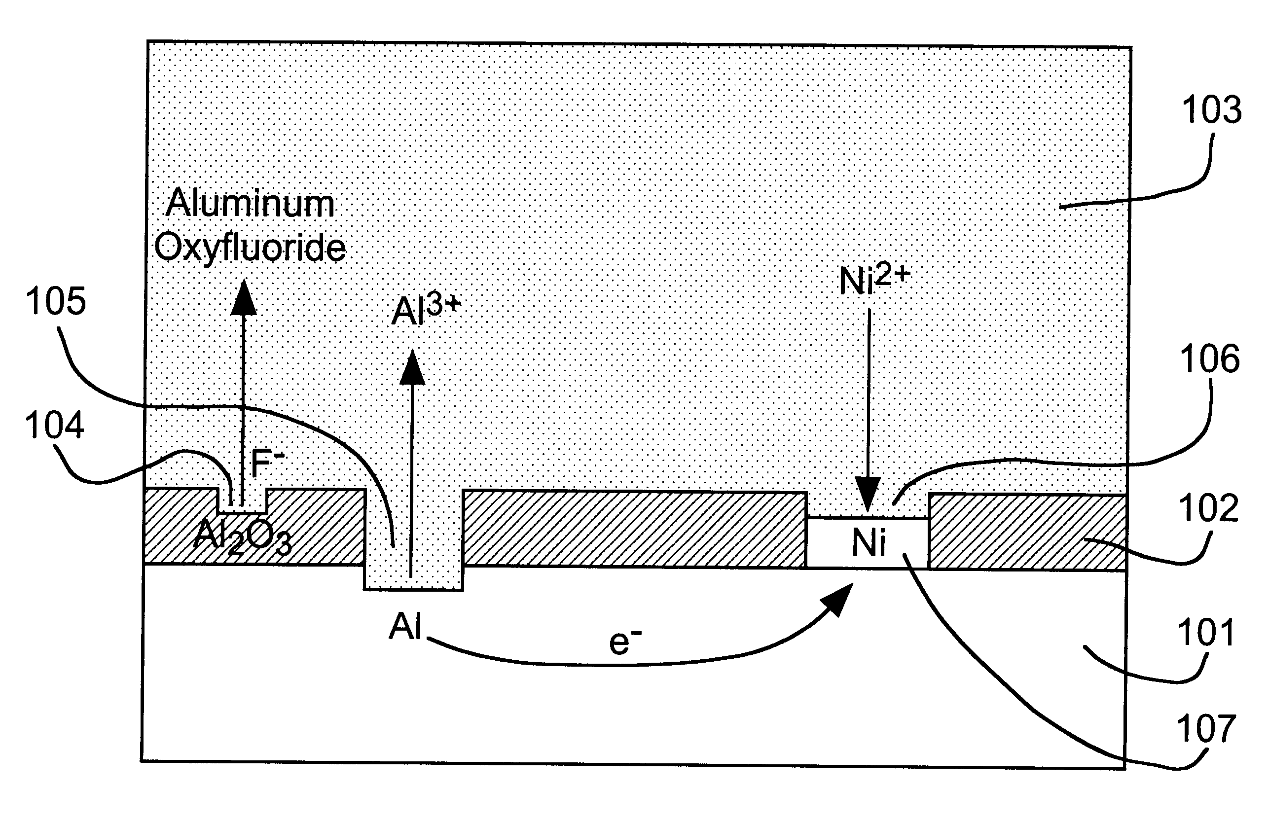
A key novel feature of the present invention is the utilization of an activator concentration gradient to minimize dissolution of the active metal substrate while providing practical rates for the oxide dissolution and displacement reactions. Such a concentration gradient is attained by utilizing a relatively high concentration of the displacing metal ions and a low concentration of the activator species coupled with minimized solution agitation within pores in the substrate surface oxide. Under these conditions, activator consumption in the oxide dissolution process reduces the concentration of activator species at the surface, especially within pores in the oxide layer where substrate attack by the activator occurs. Because of their relatively high concentration, the stable metal ions do not become significantly depleted so that the displacement reaction proceeds at a high rate. This also tends to minimize substrate attack by the activator species, which practically ceases once a continuous layer of the stable metal is formed. This approach involving use of a low level of solution agitation is counter to the teachings of the prior art since plating baths generally require vigorous solution agitation to avoid depletion of essential bath constituents at the part surface.
Direct displacement plating of nickel on aluminum according to this invention offers important advantages compared to the two-step process of the prior art, involving zincating from a strongly alkaline solution and subsequent displacement of the zinc layer by nickel from an electroless nickel bath. Attack of the aluminum substrate is minimized both during the displacement process and subsequently so that consumption of thin aluminum pads on IC chips is of less concern. After the uniform, adherent stable metal coating is produced, the displacement reaction practically ceases so that the process is robust, whereas the zincating reaction will continue until the pad is consumed. With the direct displacement process of this invention, attaining complete removal of the zinc displacement layer and avoiding contamination of the electroless nickel bath are not issues.

Problems solved by technology

Aluminum is widely used for circuitry patterns on integrated circuit (IC) chips but is very difficult be directly solder because it is a very reactive metal that forms a thick oxide layer, which prevents direct contact between the solder and the aluminum metal.
This thick oxide is recalcitrant in that it is difficult to remove and reforms almost instantaneously under ambient conditions.
Wire bonding imposes significant limitations for microelectronic applications.
Since the bonds are made one at a time, the process is relatively slow and expensive compared to soldering, which can form thousands of connections almost simultaneously.
The expense of the gold wire adds significantly to the costs.
Another important drawback is the inductance of the gold wires themselves, which becomes appreciable at high signal frequencies and limits device switching times or clock speeds.
Furthermore, because of wire length and routing issues, wire bonds are not practical for connecting to the area arrays, e.g., ball grid arrays, that are becoming commonplace as the sizes of IC chips decrease and clock speeds and the number of input / output (I / O) connections increases.
Such vacuum processing is inherently very expensive and also requires photoresist masking to enable lift-off of metal deposited in non-pad areas, or to confine subsequently electrodeposited metal layers to the pads.
A significant concern for electroplating processes is non-uniformity of the plated layers, especially overplating of isolated pads and underplating of those close together.
However, copper can migrate rapidly in aluminum and degrade both the mechanical properties of the aluminum and the electronic performance of the underlying silicon.
Consequently, a barrier layer, e.g., titanium / tungsten or tantalum nitride, is required between copper and silicon on IC chips, which precludes the possibility of utilizing a copper displacement process.
Furthermore, copper displacement coatings on aluminum tend to be porous and poorly adherent, and can produce rapid corrosion of the aluminum via galvanic action, so that they are only moderately effective for protecting aluminum against corrosion or serving as the basis for a corrosion-resistant overlayer.
This process for indirect displacement plating of nickel on aluminum via zincating has major drawbacks, especially for plating pads on IC chips.
One fundamental problem is that hydroxide ion in the strongly alkaline zincating solution aggressively attacks the aluminum itself with evolution of hydrogen gas (2Al+2OH.sup.- +2H.sub.2 O.fwdarw.2AlO.sub.2.sup.-+3H.sub.2).
In addition, the zinc deposit is porous and non-uniform since the displacement reaction must occur rapidly while dissolution and hydrogen evolution are also occurring on both the bare aluminum substrate and the zinc metal deposit.
Double zincating consumes even more aluminum and only partially improves the zinc deposit quality.
Furthermore, poor adhesion of the nickel deposit results if the zinc deposit is not completely removed by dissolution in the electroless nickel bath, which is difficult to ensure.
Another fundamental problem with the overall process is the use of an electroless nickel bath for both the nickel / zinc displacement and electroless deposition reactions, which have dichotomous requirements.
In particular, strongly complexed nickel ions should provide better quality deposits by slowing the displacement reaction to a moderate rate, but would not be reducible by the mild reducing agents needed to avoid extraneous electroless deposition.
Buildup of zinc ions in the electroless nickel plating bath can also degrade the deposit quality.
It is not surprising that such a dynamic process with many uncontrollable variables has not produced consistent results in production use.
A method for direct displacement plating of nickel on aluminum might be expected to yield the high quality deposits needed for a practical IC chip bumping process but has not been developed previously despite the long standing need.
One reason is that the hydroxide ion employed in the prior art to remove the aluminum surface oxide in the zincating process cannot be used in a nickel displacement plating solution since it would precipitate nickel hydroxide, which is highly insoluble.
Note that nickel forms amine complexes in aqueous solution that are stable in the presence of hydroxide ion but these do not allow nickel displacement plating on aluminum.
The situation is further complicated because of the relatively low activity of nickel for displacement reactions.
Degradation in wire bondability of aluminum pads is a particular problem for low-volume IC chip users who must purchase in volume to obtain a good price and then store chips for later use.
Nonetheless, appreciable amounts of water may be present without significantly reducing the benefit provided by the nonaqueous solvent.
Excessively fast displacement plating results in porous, poorly-adherent deposits.
Under these conditions, activator consumption in the oxide dissolution process reduces the concentration of activator species at the surface, especially within pores in the oxide layer where substrate attack by the activator occurs.
This approach involving use of a low level of solution agitation is counter to the teachings of the prior art since plating baths generally require vigorous solution agitation to avoid depletion of essential bath constituents at the part surface.
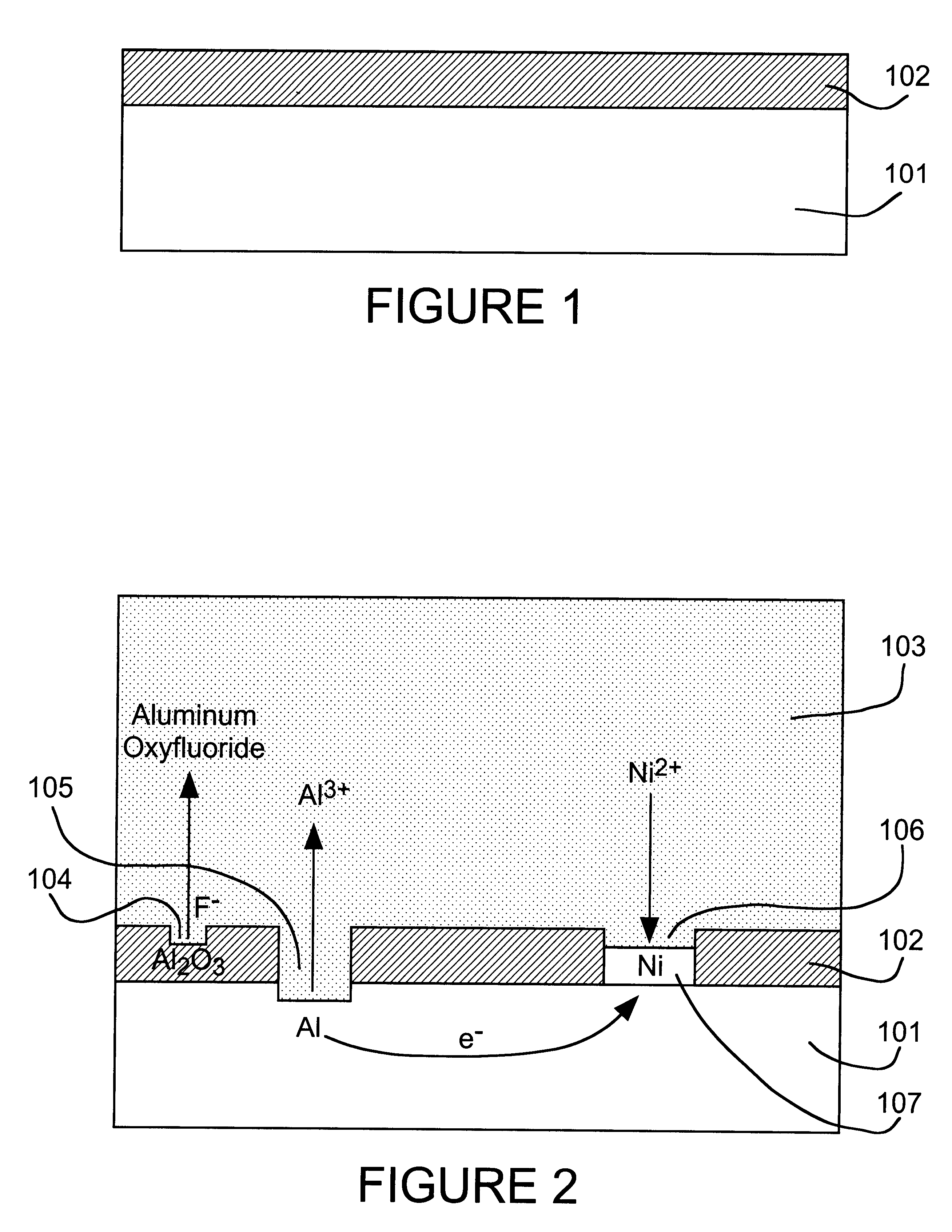
A thick surface oxide layer 102, which can result from long storage or previous processing, may be difficult to penetrate so that a sufficiently strong wire bond cannot be formed under normal wire bonding conditions.
1) a solvent, either nonaqueous, aqueous or mixtures thereof. Preferred solvents include dimethylsulfoxide (DMSO), ethylene glycol (EG), and other organic liquids. Water reacts with bare aluminum and other reactive metals with evolution of hydrogen gas, which results in excessive consumption of substrate material and may degrade the quality of the displacement coating. Deposits obtained from purely aqueous solutions may be acceptable but may not be as adherent, at least in some cases, since a slight amount of material can be removed by rubbing. Some anions containing fluorine, e.g., SiF.sub.6.sup.2-, are also unstable in aqueous solutions, which would limit the choice of activator species. In addition, the preferred DMSO and EG nonaqueous solvents are less volatile than water so that higher temperatures can be used to accelerate the rates of the oxide dissolution and displacement reactions. On the other hand, water may be present in appreciable amounts in nonaqueous systems without degrading the quality of displacement coating obtained. Insensitivity to the presence of water is highly beneficial for a practical process.
2) a fluoride activator species to dissolve surface oxide layer 102 so that the displacement reaction can occur at a practical rate. Hydroxide is used as an activator for the zincating process of the prior art but has been found to be too aggressive and difficult to control, and typically cannot be used in anhydrous nonaqueous solvents. Hydroxide usually cannot be used for nickel displacement plating since Ni(OH).sub.2 is highly insoluble and would precipitate from most solutions. Nickel amine complexes are stable in the presence of hydroxide ion but do not displacement plate nickel on aluminum. The fluoride activator of the present invention can be added as a simple fluoride salt or in the form of an complex fluoroanion, which yields fluoride by dissociation. Based on the rate of the nickel displacement reaction on aluminum in DMSO, we have found the activity of fluoride to decrease in the order: F.sup.- >AlF.sub.6.sup.3->SiF.sub.6.sup.2->>PF.sub.6.sup.-, BF.sub.4.sup.- for various anion sources.
3) ions of the relatively stable metal to be deposited by displacement plating on the reactive metal. Nickel, cobalt and palladium are relatively oxidation-resistant and can be used as solderable finishes for electronics applications. Displacement coatings of all three metals have been applied to aluminum substrates by the displacement process of the present invention. A thin overlayer of noble metal, e.g., gold, may be used to preserve the solderability and wire bondability of nickel and cobalt coatings. The preferred solution anions are halides (chloride, bromide and iodide) or pseudohalides (cyanide and thiocyanate), which tend to beneficially inhibit the displacement process by complexing the stable metal ions and adsorbing on the metal surface. Of these, chloride and bromide are most useful, since complexes of other halide and pseudohalide anions tend to lack sufficient solubility or stability, or form overly stable complexes that would slow the displacement reaction excessively.
This is particularly true when surface oxide 102 has become excessively thick, nonuniform or contaminated by prior processing, long storage and / or exposure to corrosive or contaminated environments.
Pretreatment of aluminum pads on IC chips in this solution at 50.degree. C. for 5 to 10 seconds yielded more uniform displacement coatings for chip batches that tended to give poor results, whereas pretreatment in this solution was ineffective at room temperature and resulted in excessive etching of the aluminum at 100.degree. C.
This is particularly important for high volume production processes for which buildup of high concentrations of contaminants can interfere with the functioning of the treatment solutions.
Water present in such nonaqueous solvents is apparently not detrimental but use of pure water as the solvent does not produce the best displacement coatings.
The reactivity of the activator must be sufficiently high that the rate-limiting oxide dissolution step is fast enough for a practical process, but not so high that excessive substrate dissolution occurs through pores in the oxide.
In addition, the inherent reactivity of the stable metal ions must be high enough that the displacement reaction keeps up with the oxide dissolution reaction, but must not be so high that the displacement process is uncontrolled and produces powdery deposits.
In principle, laminar solution flow or part movement parallel to the surface could enhance solution mass transport to the surface without perturbing the solution in pores but can be difficult to attain uniformly over the part surface and to maintain constant with time.

Method used


Image

  • Controlled plating on reactive metals
  • Controlled plating on reactive metals
  • Controlled plating on reactive metals

Examples


example 1

A mixture containing 5.2 g of anhydrous NiCl.sub.2 (2.0 M) and 0.25 g of Ni(en).sub.3 SiF.sub.6 (0.03 M) in 20 mL of DMSO was stirred in a 50 mL beaker on a hotplate set at 120.degree. C. until all of the solid material dissolved. The stir bar was removed from the hot solution and a silicon IC test chip with evaporated aluminum pads was placed face up in the bottom of the beaker. After 10 minutes in the quiescent solution (at approximately 100.degree. C.) the chip was removed, rinsed thoroughly with water, and quickly placed into a stirred electroless Ni plating bath for 20 minutes. The chip was then rinsed thoroughly with water and placed in an immersion Au bath for 15 minutes. The aluminum pads on the chip were uniformly coated with adherent layers of nickel and gold, as observed microscopically. At room temperature, some of the NiCl.sub.2 crystallized from the displacement plating solution but redissolved upon heating.

example 2

In the same way as in example 1, a silicon IC test chip was treated for 10 minutes in a quiescent EG solution containing 2.0 M NiCl.sub.2 and 0.03 M [(CH.sub.3).sub.4 N].sub.2 SiF.sub.6 (at about 100.degree. C.), and then successively in electroless nickel and immersion gold baths. As in example 1, the chip pads were uniformly coated with adherent layers of nickel and gold. At room temperature, the NiCl.sub.2 remained in solution.

example 3

In the same way as in example 1, a silicon IC test chip was treated for 10 minutes in a quiescent DMSO solution containing 2.0 M CoCl.sub.2 and 0.03 M [(CH.sub.3).sub.4 N].sub.2 SiF.sub.6 (at about 100.degree. C.), and then successively in electroless nickel and immersion gold baths. The chip pads were uniformly coated with adherent layers of cobalt, nickel and gold, as observed microscopically.


PUM

PropertyMeasurementUnit
molar concentrationaaaaaaaaaa
temperatureaaaaaaaaaa

Abstract

A direct displacement plating process provides a uniform, adherent coating of a relatively stable metal (e.g., nickel) on a highly reactive metal (e.g., aluminum) that is normally covered with a recalcitrant oxide layer. The displacement reaction proceeds, preferably in a nonaqueous solvent, as the oxide layer is dissolved by a fluoride activator. Halide anions are used to provide high solubility, to serve as an anhydrous source of stable metal ions, and to control the rate of the displacement reaction. A low concentration of activator species and little or no solution agitation are used to cause depletion of the activator species within pores in the surface oxide so that attack of the reactive metal substrate is minimized. Used in conjunction with electroless nickel deposition to thicken the displacement coating, this process can be used to render aluminum pads on IC chips solderable without the need for expensive masks and vacuum deposition operations. Such coatings can also be used to preserve or restore wire bondability, or for corrosion protection of aluminum and other reactive structural metals and alloys. A thin layer of immersion gold can be used to protect the thickened coating from oxidation. The solderable aluminum IC chip pads provide the basis for a maskless bumping process for flip chip attachment.

Description

This invention is concerned with plating highly reactive metals, such as aluminum and its alloys, with more stable metals, such as nickel, that provide enhanced solderability, bondability and corrosion resistance.DESCRIPTION OF THE RELATED ARTAluminum is widely used for circuitry patterns on integrated circuit (IC) chips but is very difficult be directly solder because it is a very reactive metal that forms a thick oxide layer, which prevents direct contact between the solder and the aluminum metal. This thick oxide is recalcitrant in that it is difficult to remove and reforms almost instantaneously under ambient conditions. Consequently, electrical contact to aluminum IC pads is typically made by wire bonding, which utilizes a combination of ultrasonic vibration, pressure and thermal energy to cause a gold wire to penetrate the aluminum oxide layer and form a bond to the underlying metal. The other end of the gold wire is bonded to a pad on a substrate, or on a package (e.g., ball ...

Claims


Application Information

Patent Timeline
Patent Type & Authority Patents(United States)
IPC IPC(8): C23C18/31C23C18/18C23C18/42C23C18/32H01L21/288H01L21/60
CPCC23C18/32C23C18/54H01L21/288H01L24/11C23C18/42C23C18/1653C23C18/1651H01L2224/13099H01L2924/01004H01L2924/01012H01L2924/01013H01L2924/01015H01L2924/01016H01L2924/01022H01L2924/01027H01L2924/01029H01L2924/0103H01L2924/01039H01L2924/01046H01L2924/01073H01L2924/01074H01L2924/01075H01L2924/01077H01L2924/01078H01L2924/01079H01L2924/04953H01L2924/14H01L2924/30107H01L2924/01005H01L2924/01006H01L2924/01033H01L2924/01044H01L2924/01045H01L2924/01072H01L2924/01076H01L2924/014H01L2924/10253H01L2924/00H01L2224/45144
Inventor TENCH, D. MORGANWARREN, JR., LESLIE F.WHITE, JOHN T.
Owner CALLAHAN CELLULAR L L C
Learn More