Acidic treatment liquid and method of treating copper surfaces

Inactive Publication Date: 2006-12-26
ATOTECH DEUT GMBH
View PDF22 Cites 6 Cited by
  • Summary
  • Abstract
  • Description
  • Claims
  • Application Information

AI Technical Summary

Benefits of technology

[0056]The problems encountered if conventional means are used can be eliminated if the treatment liquid according to the present invention is used. Especially the adhesion of organic films being subsequently applied to the copper surfaces may be improved. For this purpose a small etching off of copper is required only, the copper thickness therefore varying only in a narrow range after the etching process has been carried out. For this reason impedance-controlled printed circuit boards may be manufactured. Furthermore the light color of copper is conserved during the treatment. Therefore problems encountered during alignment of a photomask on the conductor line pattern do not occur. Disadvantageous effects due to further processing of the copper surfaces exposed after the organic film has been removed, for example due to electroless plating of tin, silver, nickel, gold or palladium or due to depositing organic protective coatings prior to soldering, have not been observed.
[0057]It has proven that a high adhesion of the organic films to the copper surfaces can be achieved even after a small etching off of copper if a certain copper structure is formed during the etching method. If the conventional mechanical roughening techniques of grinding or pumicing as well as if conventional chemical etching methods using solutions, simply containing hydrogen peroxide and sulfuric acid, are applied, surface structures on the copper surfaces are formed due to roughening which are too large or too even, so that adhesion of very narrow conductor lines and extremely fine solder pads and bond pads is not sufficiently high to exclude lifting off or flaking of the film due to mechanical, chemical or thermal strain. Very fine microstructures are formed on the copper surfaces if the etching means according to the present invention is used, the microstructures guaranteeing high adhesion. High adhesion may in fact also be achieved if a few of the aforementioned chemical etching means is used which contain hydrogen peroxide and an inorganic acid. However, in general very rough surfaces are generated. For example it has proven that deep cracks (depth of 1–5 microns) are formed in the copper surfaces if the method described in EP 0 890 660 A1 is applied. On the contrary the structures on the copper surfaces obtainable with the method according to the present invention have two orders of irregularities having different structural dimensions: On the one hand semicrystalline structures are formed which—dependent on the crystallite size in the copper surfaces—have an average size in the range of from 1–10 microns. If the copper surfaces would exclusively have structural dimensions of this size adhesion of the films would not be sufficiently high on the surfaces. On the other hand pits and dendritic structures are generated due to the use of the microstructure modifying agents according to the present invention the pits and dendritic structures having an average size in the range of from 50–500 nanometers and superponing the semicrystalline structures. The average sizes of the two types of irregularities are structure widths in the copper surfaces that are averaged over an area of 1 micron×1 micron (1 μm2). As the structure widths the widths of individual peaks and valleys are determined by evaluating SEM (Scanning Electron Microscope) photographs.
[0058]Furthermore if conventional methods are used considerable etching off of copper takes place. In contrast thereto it is not necessary to etch off more than 1.5 microns of copper, preferably not more than 1.0 micron, if the method according to the present invention is applied in order to guarantee sufficiently high adhesion of the organic films to the copper surfaces. This property of the treatment liquid according to the present invention is of exceptional importance if electric circuits having smaller and smaller size of the conductor lines as well as of the solder pads and bond pads are to be manufactured. Due to the minor etching off of copper manufacture of impedence-controlled circuits is made possible for which conductor line cross-section must be be kept within a narrow range of tolerance.
[0059]Besides it has been observed that the copper surfaces darken if any of a plurality of conventional chemical etching methods is applied so that safe alignment of a photomask with respect to the conductor pattern is no longer possible. If the treatment liquid according to the present invention is used a mat, light and copper-colored copper surface is formed. Alignment may therefore easily be carried out since alignment is facilitated considerably due to the high contrast between the light copper surfaces and the substrate surface.
[0060]Subsequent chemical treatment of copper surfaces exposed again after organic films had been applied thereto is possible without loss of production safety if the method according to the invention is used as opposed to conventional methods. If the conventional methods are used problems encounter frequently, for example when tin, silver, nickel, gold or palladium are deposited in an electroless manner or when organic protective coatings are applied prior to soldering. These problems in part consist in that deposition of the metals mentioned cannot be achieved at all and in part consist in that just very uneven deposition is achieved. The problems further arise if the copper surfaces are pretreated with the etching means prior to depositing the organic film. These problems may possibly be ascribed to the presence of triazoles. The reason of problems arising if the exposed copper surfaces are chemically further processed is probably a thin layer of adsorbed triazoles or any other organic compound on the treated copper surfaces if conventional etching means are used. A thin adsorption layer possibly formed due to application of the method according to the present invention can however be removed easily by means of alkaline or acidic cleaning solutions usually used in printed circuit board manufacturing processes. Because of that a subsequent metallization method, for example a method for electroless plating of tin, silver or nickel / gold or a soldering method using a slightly acidic fluxing agent, may be carried without any difficulties.
[0061]The copper surfaces are first cleaned prior to the treatment with the liquid according to the present invention in order to remove impurities from the copper surface which could impair the treatment. All conventional cleaning agents can be used. Usually surface active agents and if possible also complexing agents, such as for example triethanolamine, are added to the aqueous cleaning solutions in order to achieve an improved cleaning action.

Problems solved by technology

The aforementioned roughening methods have proven problematical in that the organic films do not have sufficient adhesion to the copper surfaces if they are deposited to the copper surfaces of very narrow conductor lines and to extremely fine solder pads or bond pads.
In further processing of the printed circuit boards treated in this manner this leads to a reduction of contrast in color between copper and the epoxy resin substrate, visual alignment of a photomask on the conductor line pattern being rendered very difficult if the alignment marks are formed by the copper surface.
On carrying out the aforementioned methods it has been observed in part that problems arise when the copper surfaces, exposed again after organic films had been applied thereto, are chemically treated, for example when tin, silver, nickel, gold or palladium are deposited in an electroless manner or when organic protective layers are applied prior to soldering.
These problems in part consist in that deposition of the metals mentioned could not be achieved at all and in part that just a very uneven deposition was formed, and the problems arise if the copper surfaces have been pretreated with the etching means prior to applying the organic film.
Using conventional methods and treatment solutions it is therefore not possible to fulfill the following requirements simultaneously:a. Sufficiently high adhesion of the organic film also on very narrow conductor lines and extremely fine solder pads and bond pads on a printed circuit board.

Method used


Image

  • Acidic treatment liquid and method of treating copper surfaces
  • Acidic treatment liquid and method of treating copper surfaces
  • Acidic treatment liquid and method of treating copper surfaces

Examples


example 1

[0075]An aqueous solution according to the present invention was prepared by mixing the following components:

[0076]

sulfuric acid, 96% by weight50mlhydrogen peroxide, 35% by weight35ml5-aminotetrazole2gL-cystine0.1gAdd up with deionized water to 1 liter.

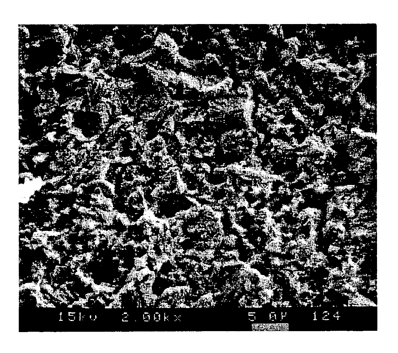
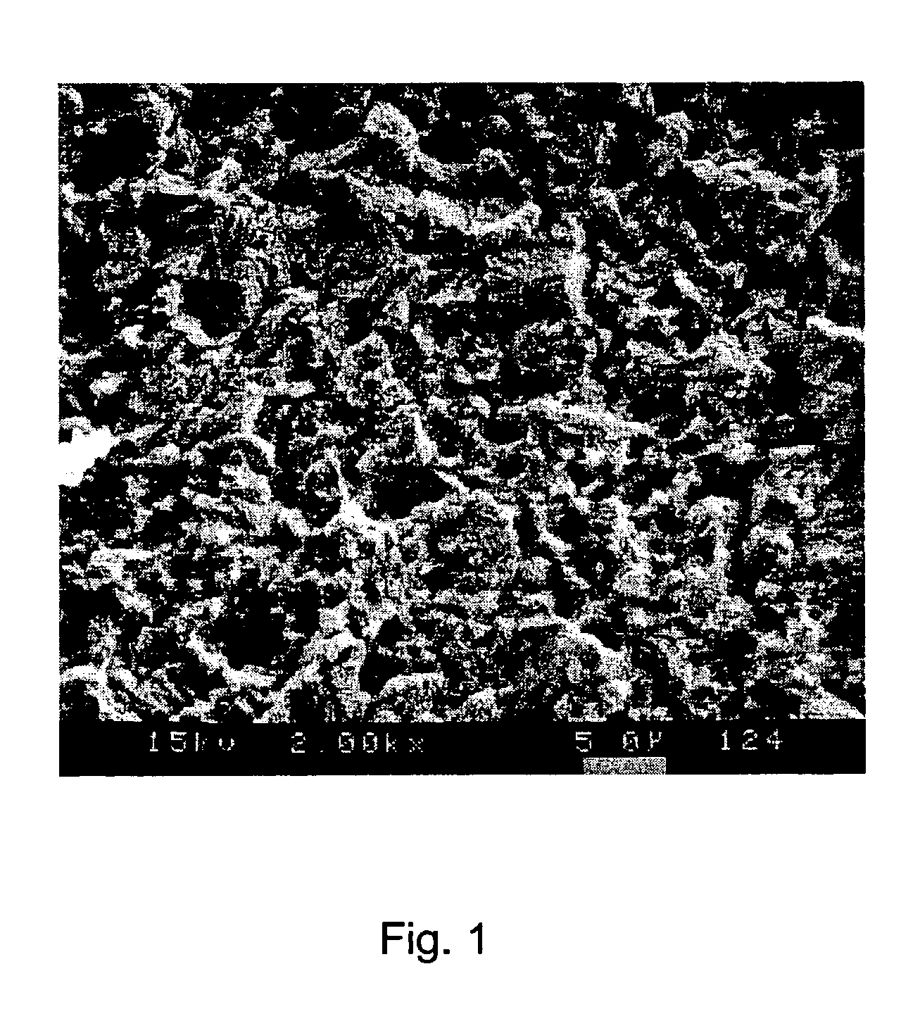
[0077]The solution was heated to 35° C. A printed circuit board, which had been plated by means of a bright copper bath (for example CUPRACID® BL-CT, sulfuric acid copper bath of Atotech Deutschland GmbH) preferably developped for the manufacture of printed circuit boards, was dipped into the solution according to the invention for 60 seconds. After treatment the copper surfaces were rinsed with warm deionized water and then dried with hot air. The copper surface obtained was mat and had a light pink color. The thickness of the copper layer etched off by means of the solution amounted to 0.9 microns. The microstructure of the copper surface exhibited two different structural (lateral) dimensions; (1) On the one hand semicrystalline st...

example 2

[0079]An aqueous treatment solution according to the present invention was prepared by mixing the following components:

[0080]

sulfuric acid, 96% by weight50mlhydrogen peroxide, 35% by weight35ml5-aminotetrazole2gthiobenzamide0.05gAdd up with deionized water to 1 liter.

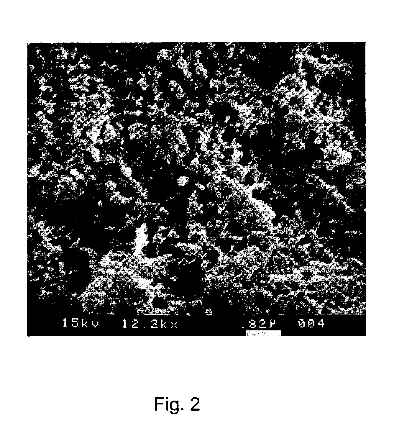
[0081]The solution was heated to 35° C. for carrying out the method. A copper substrate which was prepared using CUPRACID® BL-CT was dipped into the solution for 50 seconds. After treatment the copper surfaces were rinsed with warm deionized water and then dried with hot air. The copper surface obtained was mat and had a light pink color. The thickness of the copper layer etched off by means of the solution amounted to 0.8 microns. The microstructure of the copper surface again exhibited two different structural (lateral) dimensions; (1) On the one hand semicrystalline structures were formed which had a structural size in the range of from 1–7 microns. (2) On the other hand pits and dendritic structures with a size of f...

example 3

[0083]An aqueous solution was prepared by mixing the following components:

[0084]

sulfuric acid, 96% by weight50mlhydrogen peroxide, 35% by weight35ml1H-1,2,3-triazolo [4,5-b] pyridine1.5gL-cystine0.1gAdd up with deionized water to 1 liter.

[0085]The solution was heated to 35° C. for carrying out the method. A copper substrate which was prepared using CUPRACID® BL-CT was dipped into the solution for 50 seconds. After treatment the copper surfaces were rinsed with warm deionized water and then dried with hot air. The copper surface obtained was mat and had a pink color. The thickness of the copper layer etched off by means of the solution amounted to 0.85 microns. The microstructure of the copper surface exhibited two different structural dimensions; (1) semicrystalline structures were formed which had a structural size in the range of from 4–10 microns; (2) and deep pits with a size of from 300–500 nanometers were formed within the larger semicrystalline structures.


PUM

PropertyMeasurementUnit
Densityaaaaaaaaaa
Densityaaaaaaaaaa
Densityaaaaaaaaaa

Abstract

The present invention relates to a solution and to a method of treating copper surfaces, the copper surfaces being brought into contact with an acidic treatment liquid which contains hydrogen peroxide and at least one five-membered heterocyclic compound as well as additionally at least one microstructure modifying agent selected from the group comprising thioles A, disulfides B, sulfides C and thioamides D having the following respective general formulae:wherein R1 and R2=alkyl, alkenyl, aryl, aralkyl, especially benzyl, cycloalkyl and the derivatives thereof and R3=R1, R1—O, R1—S, amino or substituted amino, wherein R1 and R2 may especially be phenyl or substituted phenyl.

Description

CROSS-REFERENCE TO RELATED APPLICATIONS[0001]This application is filed under 35 U.S.C. 371 and is the National Stage of International Application No. PCT / EP01 / 07788 filed on Jul. 6, 2001 which claims priority to German Patent Application DE10043022.9 filed Jul. 7, 2000.BACKGROUD OF THE INVENTION[0002]The invention relates to an acidic treatment liquid and to a method of treating copper surfaces, especially of forming copper surfaces on printed circuit boards, the copper surfaces being suitable for the subsequent coating with plating resists, etch resists, solder masks and other dielectric films and further to copper substrates having roughened surfaces.[0003]In the manufacture of printed circuit boards copper surfaces are coated with various organic films, such as for example etch resists, plating resists, solder masks and other dielectric materials. These films can be applied to the board surfaces as a liquid or as a dry film resist. In any case good adhesion of the film to be appl...

Claims


Application Information

Patent Timeline
IPC IPC(8): C09K13/00C23C22/52C23F1/18H05K3/06H05K3/28H05K3/38
CPCC23C22/52C23F1/18H05K3/383H05K3/064H05K3/28H05K2203/0796H05K2203/124
Inventor HAUF, UWEFUERHAUPTER, HARRYSTIOP, ALEXEYGRIESER, UDO
Owner ATOTECH DEUT GMBH
Why Eureka
Try Eureka