
Organic compound having functional groups different in elimination reactivity at both terminals, organic thin film, organic device and method of producing the same

a technology of organic compounds and functional groups, applied in the direction of organic semiconductor devices, water-setting substance layered products, instruments, etc., can solve the problems of microfabrication restriction, device properties, difficult to obtain 100% perfect crystals with polymeric materials, etc., to prevent physical exfoliation of films, high stability, and crystallization high

Inactive Publication Date: 2007-08-23
SHARP KK
View PDF4 Cites 22 Cited by
  • Summary
  • Abstract
  • Description
  • Claims
  • Application Information

AI Technical Summary

Benefits of technology

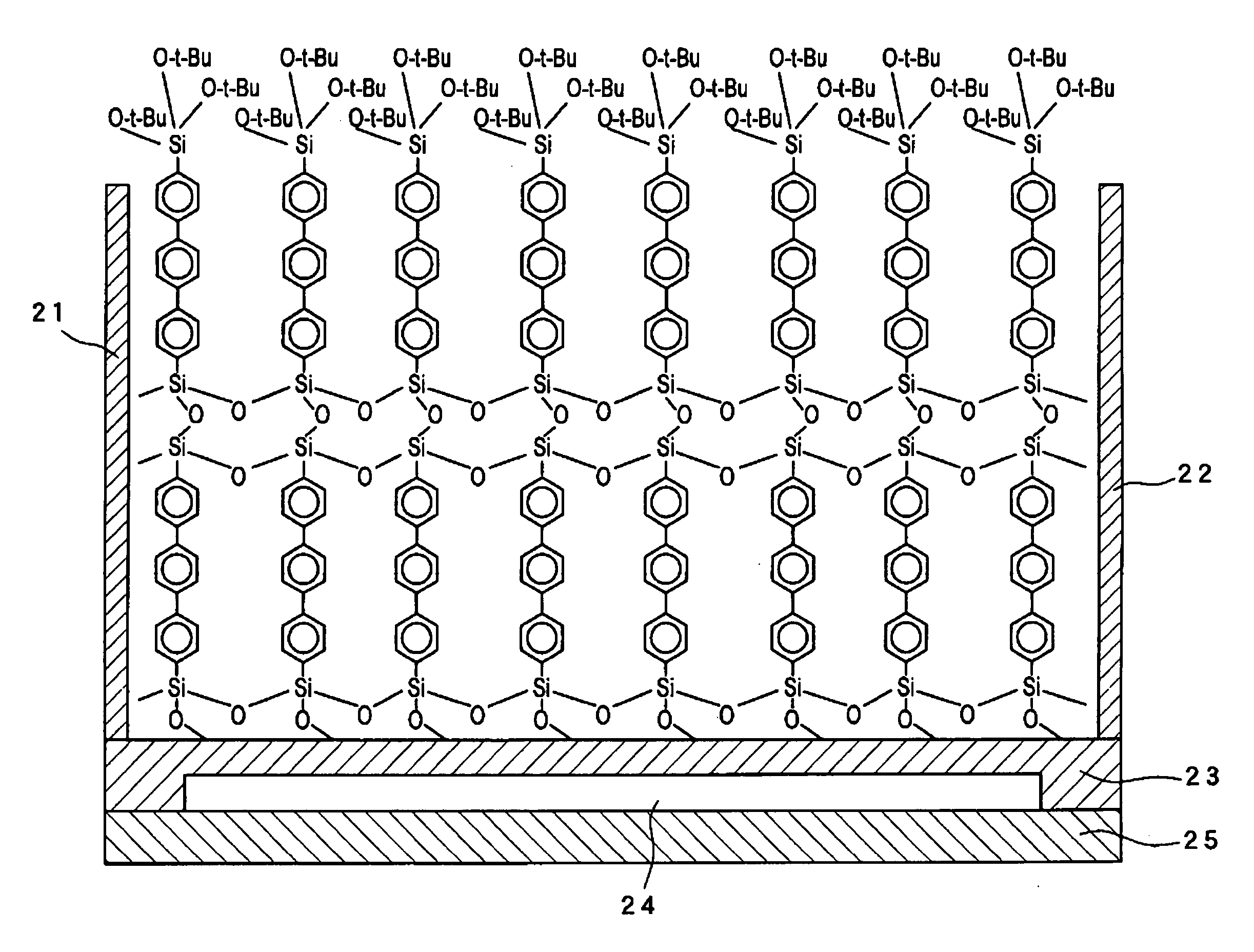
[0045] The organic compound according to the present invention provides a film highly stabilized and highly crystallized, because the film is adsorbed chemically on the substrate by the two-dimensional Si—O—Si network formed among the compound molecules and a short-distance force needed for crystallization of film, i.e., intermolecular interaction among molecules, exerts influence efficiently. Thus, the compound gives a film more tightly adsorbed on the substrate surface than the film formed on the substrate by physical adsorption, and prevents physical exfoliation of the film.
[0046] It is also possible to form an organic thin film higher in order (crystallinity) by the intermolecular interaction between the network derived from the organic compound and π-conjugated molecules, because the network derived from the organic compound constituting the organic thin film is bound directly to the organic groups. In this way, the carrier moves more smoothly by hopping conduction in the directions in parallel with and perpendicular to the molecular plane. Because the film has high conductivity also in the molecular axial direction, the film may be used widely as a conductive material not only for organic thin-film transistor material but also for solar cell, fuel cell, sensor, and the like.
[0047] In addition, such a compound can be produced easily.
[0048] It is also possible to perform adsorption on the substrate and on the film surface stepwise, selectively at high reproducibility, by varying the elimination reactivity of the groups bound to the silicon between the silyl groups that an organic compound has at both terminals, as shown in General Formula (I). Thus, the present invention provides a multilayer film more uniform in film shape and molecular orientation, at higher reproducibility than traditional methods. In other words, the present invention provides an organic thin film higher in molecule orientation in which the molecules are oriented orderly not only in the film direction but also in the film thickness direction.
[0049] When such an organic thin film is produced as a multilayer unimolecular film, the organic thin film has electrical properties different in the film thickness direction, according to the electrical properties of the constituent monomolecular layers of several nm in thickness. As a result, it is possible to control the carrier mobility efficiency, charge injection efficiency on the electrode interface, and others. In addition, the film can be applied to photo / temperature / gas sensor devices allowing high-density recording and high-speed response and / or at high sensitivity.
[0050] Further, the organic compound according to the present invention, which is self-structuring, does not demand production of an organic thin film highly crystallized and oriented under vacuum, and allows production thereof in air, which means that the production is simpler and more cost-effective, and thus, the method is advantageous as a commercial process.

Problems solved by technology

However, in the trend toward miniaturization of devices, inorganic materials, which cause crystal defects and thus have adverse effects on device properties, have restriction in microfabrication.
It is quite difficult to obtain 100% perfect crystal with a polymeric material, which has variation in molecular weight, and, among organic compounds, a low-molecular weight organic compound is normally used for such a device.
However, production of the organic compound semiconductor layer having a field-effect mobility higher than that of amorphous silicon described above demands a vacuum process such as resistance-heating vapor deposition or molecular-beam vapor deposition, making the production process more complicated, and a desirable crystalline film can be only prepared under a particular condition.
In addition, the organic compound film is adsorbed on the substrate only physically, raising a problem that the adsorption strength of the film to the substrate is weak and the film is easily exfoliated.
Further, the substrate for film formation is normally, previously processed, for example, by rubbing, for control of orientation of the organic compound molecules in a film to some extent, but there is no report yet that it is possible to control the compatibility and orientation of the compound molecules physically adsorbed at the interface between the organic compound and the substrate.
However, the electric conductivity of the self-structured film is determined by the organic functional group in the silicon compound contained in film, but there is no commercially available silane-coupling agent containing a π-electron-conjugated molecule in the organic functional group, and thus, it is difficult to provide the self-structured film with conductivity.
Although it is possible to produce a self-structured film chemically adsorbed on a substrate with the compound proposed above, it was not always possible to produce a film higher in order and crystallinity and having favorable electroconductive properties for use in electronic devices such as a TFT.
Further, use of the compound proposed above as a semiconductor layer of organic TFT raised a problem of increase in off current.
On the other hand, although the compound above may be chemically adsorbed on a substrate by forming a Si—O—Si two-dimensional network and have order by intermolecular interaction among particular long-chain alkyl groups, there was a problem that the interaction between molecules is weaker and the length of the π-electron conjugation system essential for electric conductivity is very small, because the functional group, a thiophene molecule, contributes only to π-electron conjugation system.
Even if the number of the functional groups, thiophene molecules, is increased, it is difficult to make the film-ordering factor have harmonized intermolecular interactions with the long-chain alkyl and thiophene groups.
As for electroconductive properties, such a compound had a problem that the HOMO-LUMO energy gap of the functional group, a thiophene molecule, was greater, prohibiting the compound to show sufficient carrier mobility even if it is used in TFT as an organic semiconductor layer.
In addition, when a multilayered monomolecular film (multilayer film) is formed on a substrate by chemical adsorption by using a terminal silyl group-containing silicon compound, there was a problem in the reactivity of the terminal silyl group.
Thus, it was difficult to form a multilayer unimolecular film uniform in film thickness and higher in crystal-orientation order, at high reproducibility by chemical adsorption with the conventional compound.

Method used


Image

  • Organic compound having functional groups different in elimination reactivity at both terminals, organic thin film, organic device and method of producing the same
  • Organic compound having functional groups different in elimination reactivity at both terminals, organic thin film, organic device and method of producing the same
  • Organic compound having functional groups different in elimination reactivity at both terminals, organic thin film, organic device and method of producing the same

Examples


experimental example 1

Preparative Example 1

Preparation of Disilylated Quarterthiophene Represented by Formula (a1) (Hereinafter, Referred to as Thiophene (a1))

[0260]

[0261] 2,21-Bithiophene (492-97-7) was chlorinated by treatment with NBS and chloroform in acetic acid (intermediate 1). The chlorinated bithiophene molecules were bound to each other directly at the chlorinated sites in reaction of the chlorinated bithiophenes in DMF solvent in the presence of a catalyst tris(triphenylphosphine)nickel ((PPh3) 3Ni), to give quarterthiophene.

[0262] 300 ml of a mixture solution containing 1 equivalence of quarterthiophene and 1 equivalence of triethoxybromosilane (in hexane / diethylether) was placed in a 1-liter glass flask under dry nitrogen stream; 1 equivalence of t-butyllithium was added dropwise from a funnel at −70° C. over 12 hours; and the mixture was heated once to room temperature after dropwise addition and cooled again to −196° C. Distillation of the reaction solution gave a colorless liquid of tr...

example 1

Preparation of Single Film of a Thiophene (a1) Monomolecular Film, Single Film of a Thiophene (a12) Monomolecular Film, and Bilayer Film of a Thiophene (a1) Monomolecular Film and a Thiophene (a12) Monomolecular Film

[0276] A Si wafer, quartz glass substrate, was immersed in a mixed solution of (hydrogen peroxide / sulfuric acid) and irradiated with UV light for hydrophilizing treatment, and then, washed thoroughly and cleaned with purified water, to give a substrate. Films were formed on the substrate thus obtained.

[0277] First, a toluene solution of 0.2 mM thiophene (a1) was spread on the surface of water at pH 7, allowing adsorption thereof onto the substrate associated with release of chlorine atoms of the trichlorosilyl group by the LB method, to form a thiophene (a1) monomolecular film.

[0278] Separately, a thiophene (a12) monomolecular film was formed in a similar manner to the method above, except that thiophene (a12) was used and the pH of the lower water layer was adjusted ...

example 2

Preparation of a Single Film and Bilayer to Pentalayer Films of Thiophene (a1) Monomolecular Film

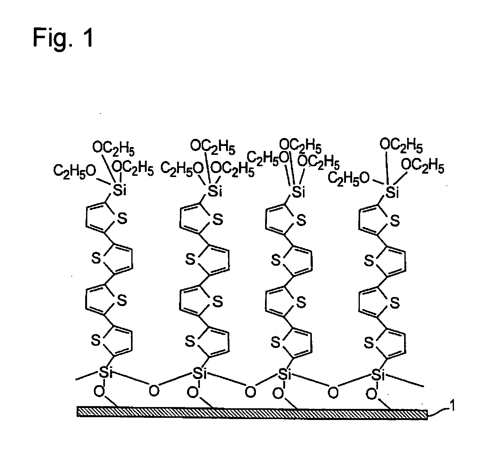
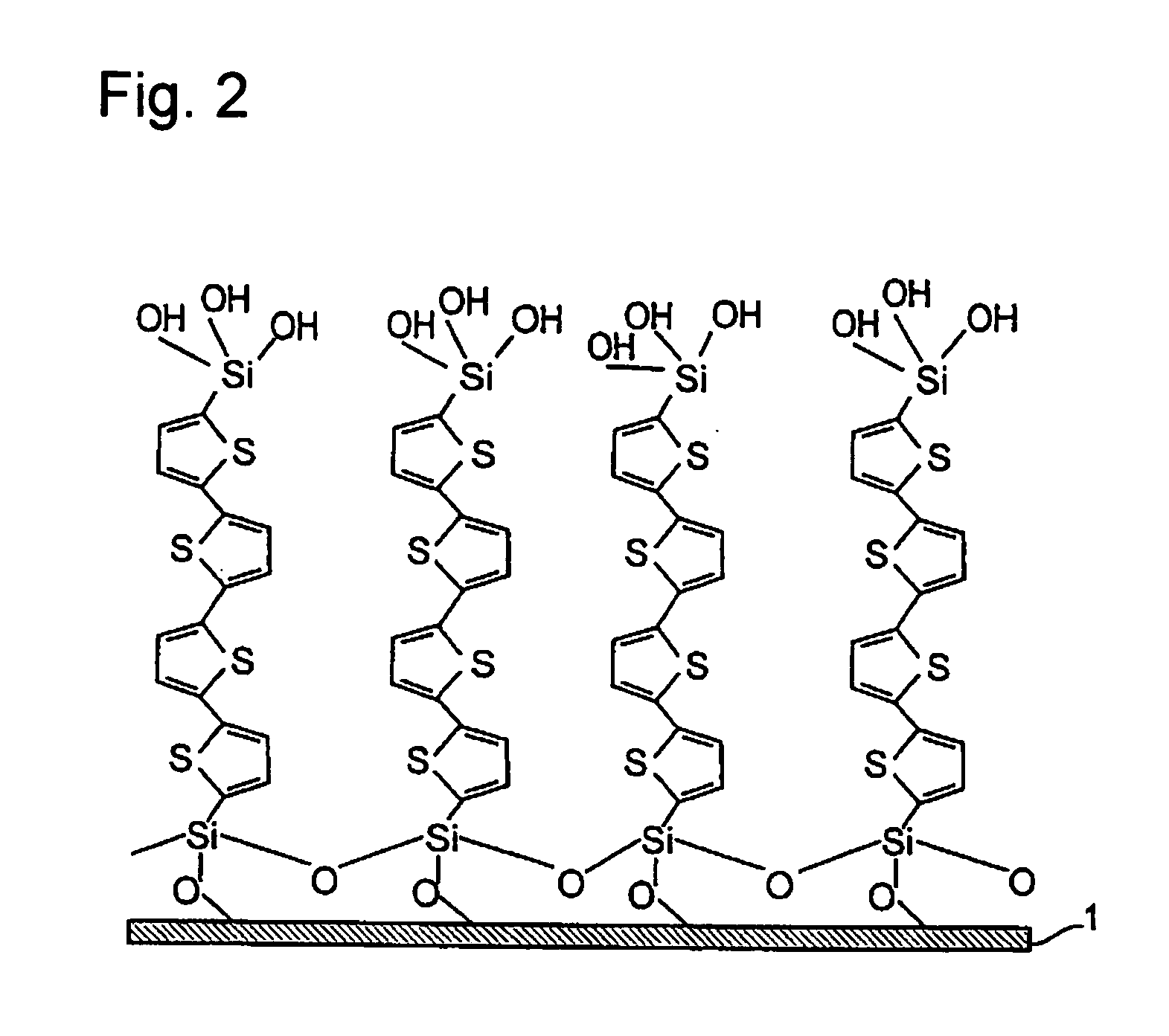
[0283] The hydrophilic substrate prepared by the method described in Example 1 was immersed in a toluene solution of 0.01 mM thiophene (a1) at room temperature for 12 hours. A monomolecular film of the bottom layer was formed, by adsorption of the thiophene (a1) molecule in reaction of the hydroxyl groups present on the substrate surface and trichlorosilyl groups. The substrate obtained was cleaned with an organic solvent for removal of the residual unreacted thiophene (a1). The cleaned substrate was immersed in purified water at pH 4, hydrolyzing the triethoxysilyll groups into trihydroxysilyl groups. Then, the monomolecular film-formed substrate ended by the hydroxysilyl-group terminal was immersed in a toluene solution of 0.01 mM thiophene (a1) at room temperature for 12 hours. The second-layer monomolecular film was formed on the monomolecular film of bottom layer, in adsorption rea...


PUM

PropertyMeasurementUnit
intermolecular distanceaaaaaaaaaa
temperatureaaaaaaaaaa

Abstract

Provided are a single monomolecular film uniform in film thickness and highly ordered in molecule alignment and its multilayer film, an organic compound allowing production of such films at high reproducibility, an organic device superior in electroconductive properties and a method of producing the same. An organic compound represented by Formula:Si(A1)(A2)(A3)-B—Si(A4)(A5)(A6)(A1 to A6 each represent a hydrogen atom, a halogen atom, an alkoxy group or an alkyl group and satisfy the relationship in elimination reactivity of: A1 to A3>A4 to A6; and B represents a bivalent organic group), an organic thin film using the compound, and an organic device having the thin film; A method of producing an organic thin film and organic device, comprising a step of forming a single monomolecular film by allowing the silyl group having A1 to A3 in the organic compound to react with the substrate surface; a step of removing unreacted organic compounds by using a non-aqueous solvent; and a step of forming an additional monomolecular film of the organic compound by using the unreacted silyl groups present on the film surface side of the monomolecular film obtained as the sites for adsorption reaction.

Description

TECHNICAL FIELD [0001] The present invention relates to an organic compound having functional groups different in elimination reactivity at both terminals, an organic thin film, an organic device, and a method of producing the same. BACKGROUND ART [0002] Inorganic materials such as a silicon crystal have been used in many semiconductor devices. However, in the trend toward miniaturization of devices, inorganic materials, which cause crystal defects and thus have adverse effects on device properties, have restriction in microfabrication. [0003] Recently, research and development on semiconductors using an organic compound (organic semiconductor) are in progress and the results have been reported, because they are simpler in production and easier in processing than semiconductors of inorganic material and compatible with expansion in size of device, and allows cost reduction by mass production, and also because it is possible to prepare organic compounds with more functions than inorg...

Claims


Application Information

Patent Timeline
Patent Type & Authority Applications(United States)
IPC IPC(8): G11C17/00B05D7/00B05D1/36B32B13/04C07F7/04C09K11/06H01L29/786H01L31/04H05B33/14H05B33/22H10K99/00
CPCH01L51/0012H01L51/005H01L51/0052H01L51/0056H01L51/0068H01L2251/308H01L51/0094H01L51/0512H01L51/0545H01L51/424H01L51/5012H01L51/0075H10K71/191H10K85/60H10K85/624H10K85/655H10K85/701H10K85/615H10K85/40H10K10/462H10K10/466H10K30/20H10K50/11H10K2102/103H10K30/50
Inventor IMADA, HIROSHIHANATO, HIROYUKITAMURA, TOSHIHIRO
Owner SHARP KK
Learn More