Composite patterning devices for soft lithography

a technology of soft lithography and composite patterning, which is applied in the direction of photomechanical treatment originals, instruments, photomechanical equipment, etc., can solve the problems of limiting the application of nanolithographic methods to a very narrow range of specialized materials, high volume processing of nanomaterials, and high cost of nanolithographic methods. achieve high resolution, good placement accuracy, and high fidelity over large substrate surface areas

Active Publication Date: 2007-03-27
THE BOARD OF TRUSTEES OF THE UNIV OF ILLINOIS
View PDF95 Cites 504 Cited by
  • Summary
  • Abstract
  • Description
  • Claims
  • Application Information

AI Technical Summary

Benefits of technology

[0015]The present invention provides methods, devices and device components for fabricating patterns on substrate surfaces, particularly patterns comprising structures having microsized and / or nanosized features of selected lengths in one, two or three dimensions. Specifically, the present invention provides stamps, molds and photomasks used in soft lithography fabrication methods for generating high resolution patterns of structures on flat and contoured surfaces, including surfaces having a large radius of curvature on a wide variety of substrates, including flexible plastic substrates. It is an object of the present invention to provide methods and devices for fabricating three-dimensional structures having well defined physical dimensions, particularly structures comprising well defined features having physical dimensions on the order of 10s of nanometers to 1000s of nanometers. It is another object of the present invention to provide methods, devices and device components for fabricating patterns of structures characterized by high fidelity over large substrate surface areas and good placement accuracy. It is further an object of the present invention to provide composite patterning devices which exhibit better thermal stability and resistance to curing induced pattern distortion than conventional single layer or multilayer stamps, molds and photomasks. It is another object of the present invention to provide soft lithography methods, devices and device components that are compatible with existing high speed commercial printing, molding and embossing techniques, devices and systems.
[0016]In one aspect, the present invention provides patterning devices comprising a plurality of polymer layers each having selected mechanical properties, such as Young's Modulus and flexural rigidity, selected physical dimensions, such as thickness, surface area and relief pattern dimensions, and selected thermal properties, such as coefficients of thermal expansion, to provide high resolution patterning on a variety of substrate surfaces and surface morphologies. Patterning devices of this aspect of the present invention include multilayer polymer stamps, molds and photomasks useful for a variety of soft lithographic patterning applications including contact printing, molding and optical patterning. In one embodiment, discrete polymer layers having different mechanical properties, physical dimensions and thermal properties are combined and / or matched to provide patterning devices having cumulative mechanical and thermal properties providing enhanced pattern resolution and fidelity, and improved thermal stability over conventional soft lithography devices. In addition, patterning devices of the present invention comprising a combination of discrete polymer layers tolerate a wide variety of device configurations, positions and orientations without fracture which make them more easily integrated into existing commercial printing, molding and optical patterning systems than conventional single layer or multiple layer stamps, molds and photomasks.

Problems solved by technology

Although nanolithography provides viable methods of fabricating structures and devices having nanometer dimensions, these methods have certain limitations that hinder their practical integration into commercial methods providing low cost, high volume processing of nanomaterials.
First, nanolithographic methods require elaborate and expensive steppers or writing tools to direct light, electrons and / or ions onto photoresist surfaces.
Second, these methods are limited to patterning a very narrow range of specialized materials, and are poorly suited for introducing specific chemical functionalities into nanostructures.
Third, conventional nanolithography is limited to fabrication of nanosized features on small areas of ultra-flat, rigid surfaces of inorganic substrates and, thus is less compatible with patterning on glass, carbon and plastic surfaces.
Finally, fabrication of nanostructures comprising features having selectable lengths in three dimensions is difficult due to the limited depth of focus provided by nanolithographic methods, and typically requires labor intensive repetitive processing of multilayers.
Although conventional PDMS patterning devices are capable of establishing reproducible conformal contact with a variety of substrate materials and surface contours, use of these devices for making features in the sub −100 nm range are subject to problems associated with pressure induced deformations due to the low modulus (3 MPa) and high compressibility (2.0 N / mm2) of conventional single layer PDMS stamps and molds.
First, at aspect ratios less than about 0.3, conventional PDMS patterning devices having wide and shallow relief features tend to collapse upon contact with the surface of the substrate.
Second, adjacent features of conventional single layer PDMS patterning devices having closely spaced (
Finally, conventional PDMS stamps are susceptible to rounding of sharp corners in transferred patterns when a stamp is released from a substrate due to surface tension.
The combined effect of these problems is to introduce unwanted distortions into the patterns of materials transferred to a substrate.
Although use of conventional composite stamps and molds have improved to some degree the capabilities of soft lithography methods for generating features having dimensions in the sub-100 nm range, these techniques remain susceptible to a number of problems which hinder there effective commercial application for high throughput fabrication of micro-scale and nanoscale devices.
First, some conventional composite stamp and mold designs have limited flexibility and, thus, do not make good conformal contact with contoured or rough surfaces.
Second, relief patterns of conventional, multimaterial PDMS stamps are susceptible to undesirable shrinkage during thermal or ultraviolet curing, which distort the relief patterns on their transfer surfaces.
Third, use of conventional composite stamps comprising multilayers having different thermal expansion coefficients can result in distortions in relief patterns and curvature of their transfer surfaces induced by changes in temperature.
Fourth, use of stiff and / or brittle backing layers, such as glass and some metal layers, prevents easy incorporation of conventional composite stamps into preexisting commercial printer configurations, such as rolled and flexographic printer configurations.
Finally, use of composite stamps having transfer surfaces comprising high modulus elastomeric materials impede formation of conformal contact between a transfer surface and a substrate surface necessary for high fidelity patterning.

Method used


Image

  • Composite patterning devices for soft lithography
  • Composite patterning devices for soft lithography
  • Composite patterning devices for soft lithography

Examples


example 1

Composite Stamps for Nanotransfer Printing

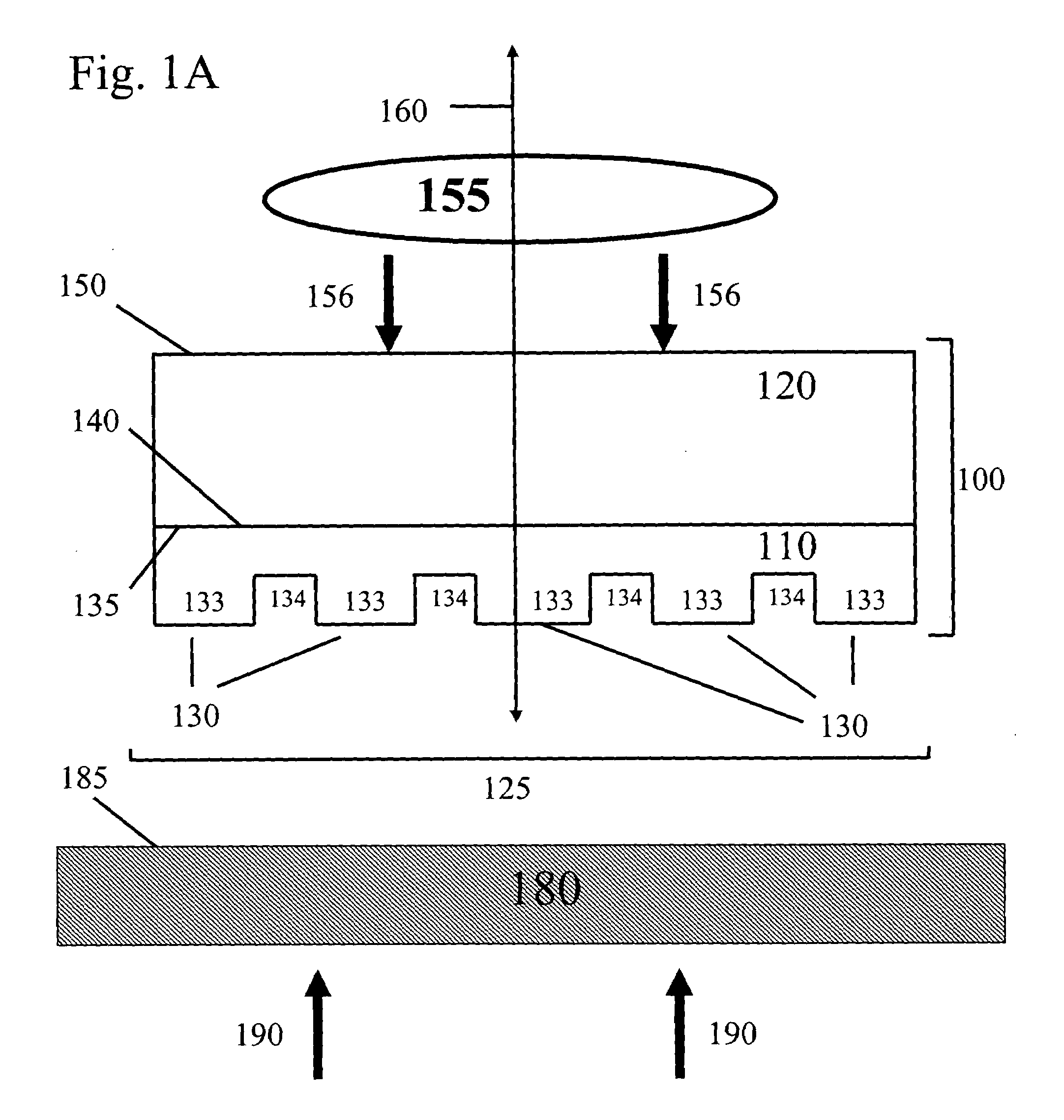
[0109]The ability of the patterning devices of the present invention to provide composite stamps for nanotransfer printing applications was verified by experimental studies. Specifically, it is a goal of the present invention to provide composite stamps capable of patterning large areas of a substrate surface with structures having selected lengths on the order of microns and 10's of nanometers. Further, it is a goal of the present invention to provide composite stamps for contact printing high resolution patterns exhibiting good fidelity and placement accuracy.

[0110]To achieve the aforementioned goals, composite stamps were fabricated using the methods of the present invention and used to generate patterns comprising monolayers of gold on substrates via nanotransfer printing (nTP). Specifically, large area composites stamps were generated and tested, comprising a thin (5–10 micron) PDMS layer in contact with a 25 micron thick polyimide (Kap...

example 2

Computer modeling of the Thermal Characteristics and Mechanical Properties of Composite Patterning Devices

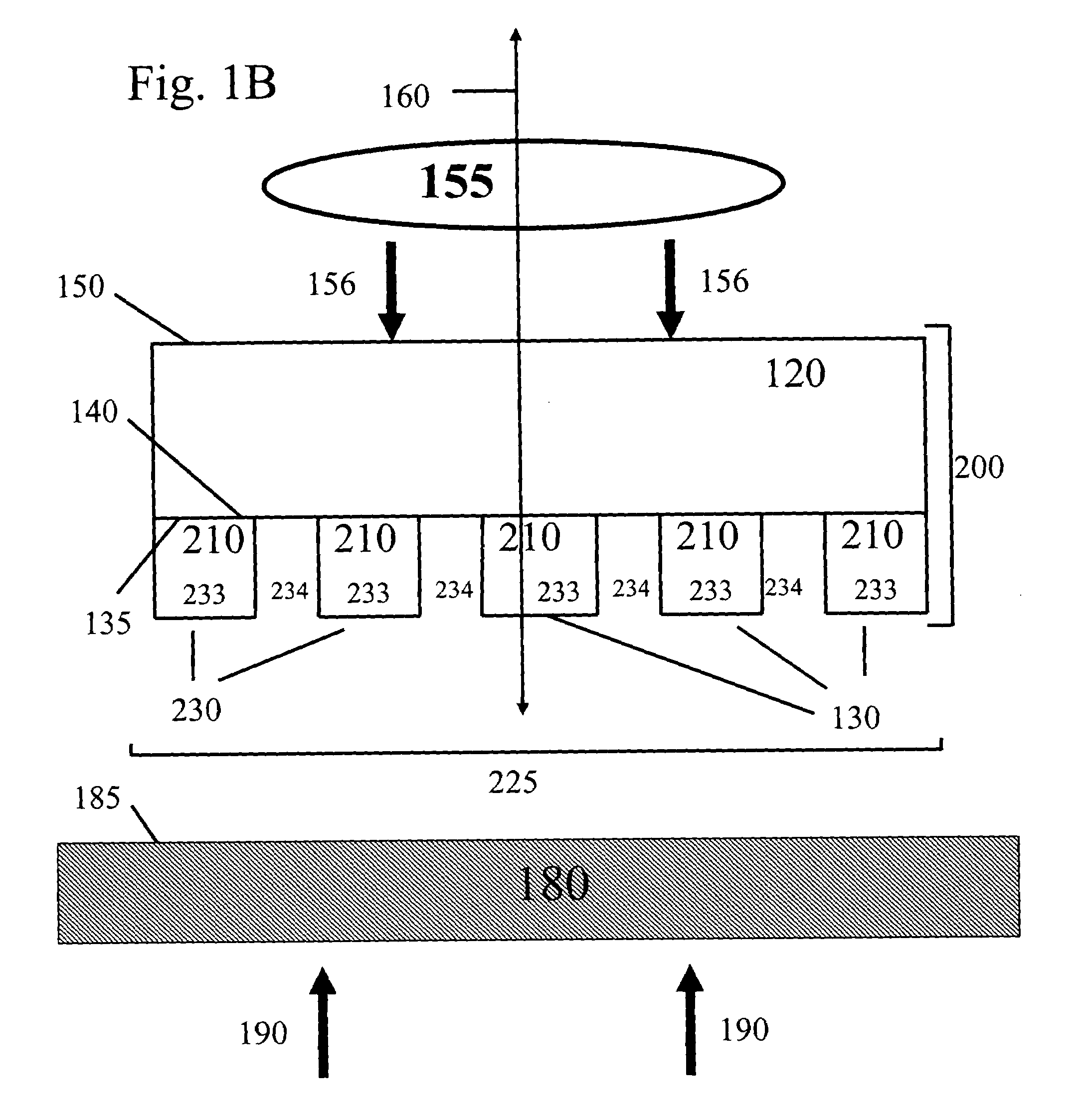
[0118]The susceptibility of multilayer patterning devices of the present invention to distortions induced by polymerization during fabrication and mechanical stresses was evaluated by computation simulations. Specifically, the extent of deformation induced by polymerization during fabrication and the weight driven deformation of recessed regions was calculated for a four layer composite patterning device. These studies verified that composite patterning devices of the present invention exhibit enhanced stability with respect to polymerization induced shrinkage and weight driven sagging.

[0119]The extent of polymerization induced distortion was calculated and compared for two different composite pattern designs. First, a four layer composite patterning device 600, shown schematically in FIG. 10, was evaluated comprising a first 5 micron thick PDMS polymer layer 610, a second 25 mi...

example 3

Fiber Reinforced Composite Patterning Devices

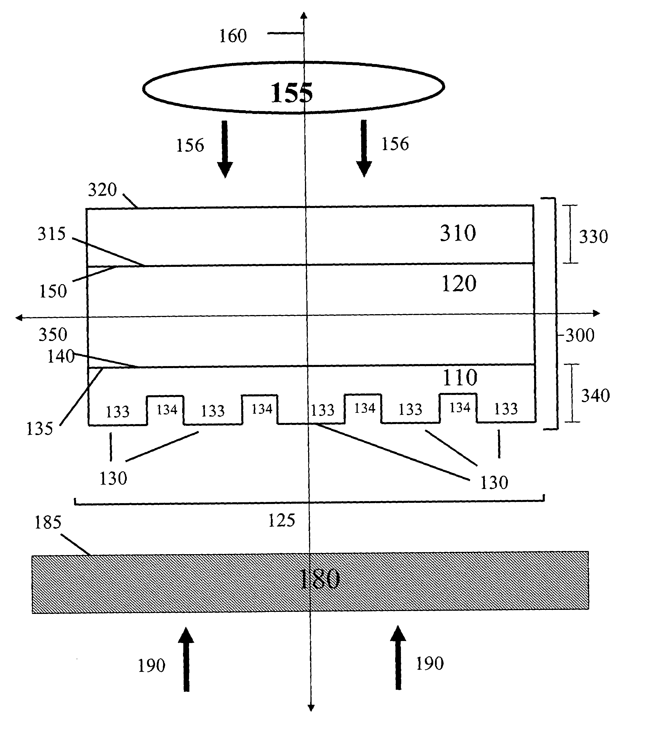
[0123]The present invention includes composite pattering devices comprising one or more composite polymer layers, including polymer layers having fiber materials providing beneficial mechanical, structural and / or thermal properties. Composite patterning devices of this aspect of the present invention include designs wherein fibers are integrated into and / or between polymer layers in geometries selected to provide a net flexural rigidity that minimizes distortion of the relief features of a relief pattern and which provide patterning devices capable of generating patterns exhibiting good fidelity and placement accuracy on substrate surfaces. Furthermore, composite patterning devices of this aspect of the present invention include designs wherein fibers are integrated into and / or between polymer layers in geometries selected to minimize expansion or contraction of polymer layers due changes in temperature and / or to facilitate physical manip...


PUM

PropertyMeasurementUnit
thicknessaaaaaaaaaa
thicknessaaaaaaaaaa
thicknessaaaaaaaaaa

Abstract

The present invention provides methods, devices and device components for fabricating patterns on substrate surfaces, particularly patterns comprising structures having microsized and / or nanosized features of selected lengths in one, two or three dimensions. The present invention provides composite patterning devices comprising a plurality of polymer layers each having selected mechanical properties, such as Young's Modulus and flexural rigidity, selected physical dimensions, such as thickness, surface area and relief pattern dimensions, and selected thermal properties, such as coefficients of thermal expansion, to provide high resolution patterning on a variety of substrate surfaces and surface morphologies.

Description

CROSS REFERENCE TO RELATED APPLICATION[0001]This application claims priority under 35 U.S.C. 119(e) to U.S. Provisional Patent Application 60 / 565,604, filed Apr. 27, 2004, which is hereby incorporated by reference in its entirety to the extent not inconsistent with the disclosure herein.STATEMENT REGARDING FEDERALLY SPONSORED RESEARCH OR DEVELOPMENT[0002]This invention was made, at least in part, with United States governmental support awarded by Department of Energy Grant DEFG02-91ER45439. The United States Government has certain rights in this invention.BACKGROUND OF INVENTION[0003]The design and fabrication of micrometer sized structures and devices have had an enormous impact on a number of important technologies including microelectronics, optoelectronics, microfluidics and microsensing. The ability to make micro-sized electronic devices, for example, has revolutionized the electronics field resulting in faster and higher performing electronic components requiring substantially...

Claims


Application Information

Patent Timeline
Patent Type & Authority Patents(United States)
IPC IPC(8): B29C67/00B29C35/08C04B24/38C04B28/14G03F7/00G03F9/00
CPCB82Y10/00B82Y40/00G03F7/0002C04B28/14C04B24/383B82Y30/00C04B2111/00181B81C1/0046
Inventor ROGERS, JOHN A.MENARD, ETIENNE
Owner THE BOARD OF TRUSTEES OF THE UNIV OF ILLINOIS
Why Eureka
Try Eureka