GaN thin film upgrowth method based on Al3O2 substrate
A thin film growth and substrate technology, applied in the field of semiconductors, can solve the problems of limiting the performance of GaN-based microwave high-power transistors, light-emitting diodes and lasers, reducing the crystal quality and critical thickness of the GaN top layer, and large changes in temperature. Small thermal stress effect, reduced linear dislocation density, reduced surface cracking effect
- Summary
- Abstract
- Description
- Claims
- Application Information
AI Technical Summary
Problems solved by technology
Method used
Image
Examples
Embodiment 1
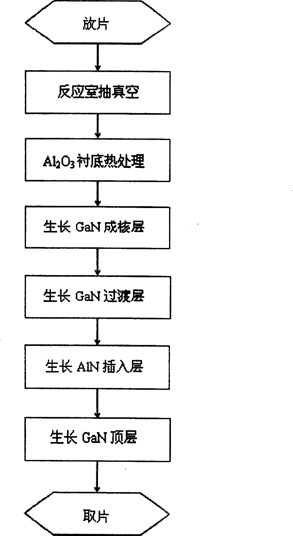
[0033] refer to figure 1 , at Al 2 o 3 Using GaN as the nucleation layer material on the substrate to grow a GaN film with a high-temperature AlN insertion layer, the specific steps are as follows:
[0034] 1. Take Al 2 o 3 The substrate is placed in the reaction chamber of the metal organic chemical vapor deposition equipment MOCVD, and the vacuum degree of the reaction chamber is pumped to 1×10 -2 Under Torr, under the protection of the mixed gas of hydrogen and ammonia, Al 2 o 3 The substrate is heat-treated, the heating temperature is 1050°C, the heating time is 5min, the pressure of the reaction chamber is 40Torr, the flow rate of hydrogen gas is 1500 sccm, and the flow rate of ammonia gas is 1500 sccm;
[0035] 2. Lower the substrate temperature to 500°C, keep the growth pressure at 40Torr, the flow rate of hydrogen gas at 1500sccm, the flow rate of ammonia gas at 1500sccm, and feed a gallium source with a flow rate of 30μmol / min into the reaction chamber to grow a...
Embodiment 2
[0040] refer to figure 1 , at Al 2 o 3 Using GaN as the nucleation layer material on the substrate to grow a GaN film with a high-temperature AlN insertion layer, the specific steps are as follows:
[0041] 1. Take Al 2 o 3 The substrate is placed in the reaction chamber of metal organic chemical vapor deposition equipment MOCVD, and the vacuum degree of the reaction chamber is evacuated to 2×10 -2 Under Torr, under the protection of hydrogen for Al 2 o 3 The substrate is heat-treated, the heating temperature is 900°C, the heating time is 10min, the pressure of the reaction chamber is 760Torr, and the flow rate of hydrogen gas is 1000sccm;
[0042] 2. Lower the substrate temperature to 400°C, keep the growth pressure at 760Torr, and the flow rate of hydrogen gas at 1000 sccm, and feed ammonia gas with a flow rate of 1000 sccm into the reaction chamber, and a gallium source with a flow rate of 1 μmol / min to grow a film with a thickness of 10 nm. Low temperature GaN nucle...
Embodiment 3
[0047] refer to figure 1 , at Al 2 o 3 Using GaN as the nucleation layer material on the substrate to grow a GaN film with a high-temperature AlN insertion layer, the specific steps are as follows:
[0048] 1. Take Al 2 o 3 The substrate is placed in the reaction chamber of the metal organic chemical vapor deposition equipment MOCVD, and the vacuum degree of the reaction chamber is pumped to 1×10 -2 Under Torr, under the protection of the mixed gas of hydrogen and ammonia, Al 2 o 3 The substrate is heat-treated, the heating temperature is 1200°C, the heating time is 8min, the pressure of the reaction chamber is 20Torr, the flow rate of hydrogen gas is 2500 sccm, and the flow rate of ammonia gas is 10000 sccm;
[0049] 2. Lower the substrate temperature to 600°C, keep the growth pressure at 20Torr, the flow rate of hydrogen gas at 2500sccm, the flow rate of ammonia gas at 10000sccm, and feed a gallium source with a flow rate of 100μmol / min into the reaction chamber to gro...
PUM
| Property | Measurement | Unit |
|---|---|---|
| thickness | aaaaa | aaaaa |
| thickness | aaaaa | aaaaa |
| thickness | aaaaa | aaaaa |
Abstract
Description
Claims
Application Information
 - R&D
- Intellectual Property
- Life Sciences
- Materials
- Tech Scout
- Unparalleled Data Quality
- Higher Quality Content
- 60% Fewer Hallucinations
Browse by: Latest US Patents, China's latest patents, Technical Efficacy Thesaurus, Application Domain, Technology Topic, Popular Technical Reports.
© 2025 PatSnap. All rights reserved.Legal|Privacy policy|Modern Slavery Act Transparency Statement|Sitemap|About US| Contact US: help@patsnap.com


