
Electrolytic device based on a solution-processed electrolyte

a technology of electrolyte and electrolysis device, which is applied in the direction of liquid/solution decomposition chemical coating, separation process, coating, etc., can solve the problems of low resistance state, high resistance, and relatively expensive and time-consuming techniques

Inactive Publication Date: 2008-12-25
GLOBALFOUNDRIES INC
View PDF3 Cites 20 Cited by
  • Summary
  • Abstract
  • Description
  • Claims
  • Application Information

AI Technical Summary

Benefits of technology

[0055]The metal or metalloid chalcogenide precursor films are deposited on a substrate using the solutions prepared as disclosed above. Suitable substrates for film deposition include: silicon, quartz, glass, sapphire, metal, gallium nitride, gallium arsenide, germanium, silicon-germanium, indium-tin-oxide, alumina (Al2O3), and plastic (e.g., Kapton, polycarbonate). The substrate may be rigid or flexible. Using high-throughput techniques such as spin-coating, stamping, dip coating, doctor blading, drop casting, or printing, solutions are applied to the substrate and transformed into thin films of the precursor upon evaporation of the solvent. Some of the solution processing techniques (e.g., printing, stamping) enable simultaneous film deposition and patterning. The key point in this step is to have chosen a solvent that will wet the appropriately prepared substrate (i.e., an oxidized silicon surface can be prepared to be either hydrophilic or hydrophobic to promote solution wetting, depending upon the nature of the solvent used), thereby facilitating the formation of a uniform film upon drying.
[0057]A low-temperature thermal treatment is used to decompose the resulting metal chalcogenide precursor film on the substrate, resulting in the formation of a metal chalcogenide amorphous film. The substrate coated with the precursor film can be heated by placing it on a hot plate, or in a box or tube furnace under an appropriate inert atmosphere such as nitrogen, forming gas or argon. Alternatively, the heating may take place by laser-based or microwave-based annealing for much more rapid processing. Heating is performed at a temperature high enough and for a time long enough to enable complete decomposition of the hydrazine-based precursor into the targeted metal chalcogenide, but low enough and for a short enough time that substantial crystallization does not occur. Preferably the heating is carried out at a temperature of about 100 to about 400° C. and more typically about 100 to about 350° C. and for an amount of time from about 0.2 to about 60 minutes. Additionally, the choice of the metal chalcogenide may be used to promote the formation of amorphous films. The particular temperatures used to obtain an amorphous film depends upon the chalcogenide precursor, which can be determined by those skilled in the art without undue experimentation in view of this disclosure. For instance, metal or metalloid chalcogenides based on the lighter metals or metalloids have less of a tendency to crystallize and therefore temperatures at the higher end of the range can be used while still maintaining an amorphous film.
[0058]Solution-based techniques are particularly attractive because of the array of available options for high-throughput film deposition, including spin coating, dip coating, doctor blading, ink-jet printing, stamping, etc. These techniques have the advantage of being potentially low-cost, high-throughput techniques and are readily compatible with roll-to-roll processing. Prior to this disclosure, the active layer was typically deposited using a slower and more costly vacuum-based technique such as sputtering or evaporation.
[0059]Advantages of this process are that it allows for potentially low-cost, very high-throughput deposition of amorphous metal chalcogenide films for use in electrolytic devices, without the requirement of vacuum conditions or specialized CVD reactors. The solution-processing technique is also a relatively low-temperature process and is compatible with selected higher-temperature flexible plastic substrate materials, such as Kapton and other polyimide-based plastics. Additionally, solution-processing provides a natural mechanism for filling vias and trenches on a substrate, which can be difficult to achieve using more directional deposition techniques such as sputtering (see U.S. patent application Ser. No. 11 / 556,385, entitled Method for Filling Holes with Metal Chalcogenides, filed Nov. 3, 2006, the disclosure of which is incorporated herein by reference). Finally, the solution processing mechanism provides a convenient means of doping the amorphous metal chalcogenide layer, since the corresponding dopant metal can be dissolved in the solution with the targeted metal chalcogenide prior to solution processing (i.e., without the need for UV diffusion).
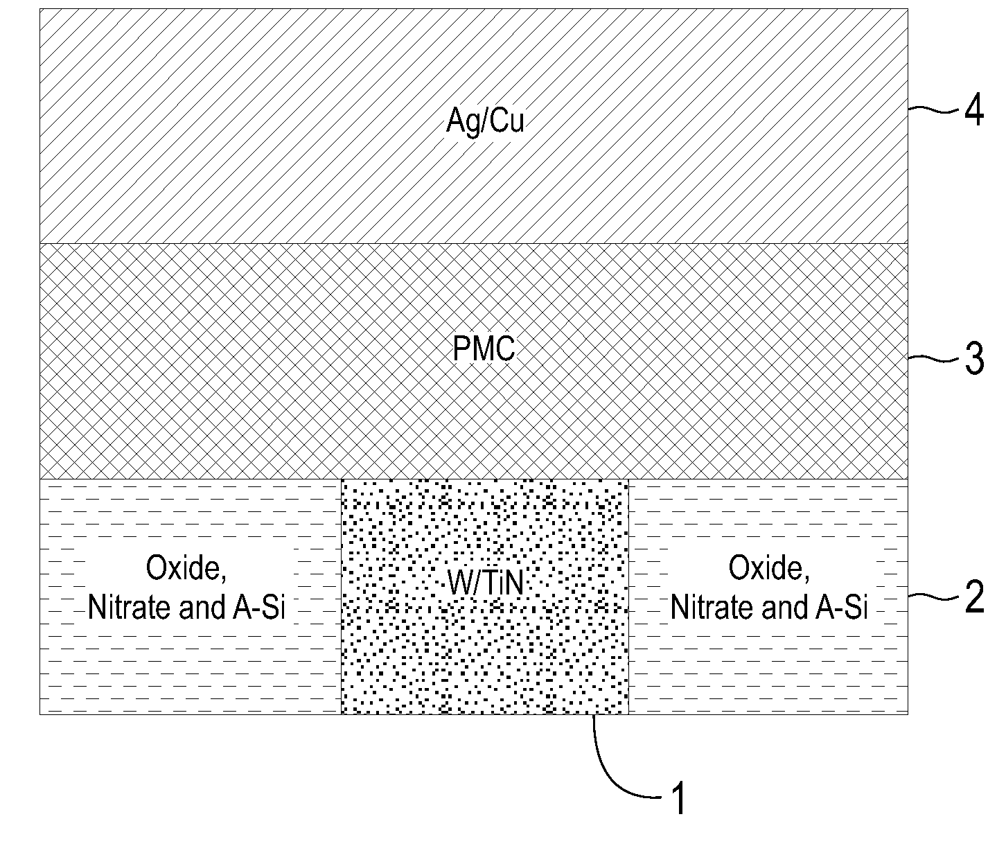
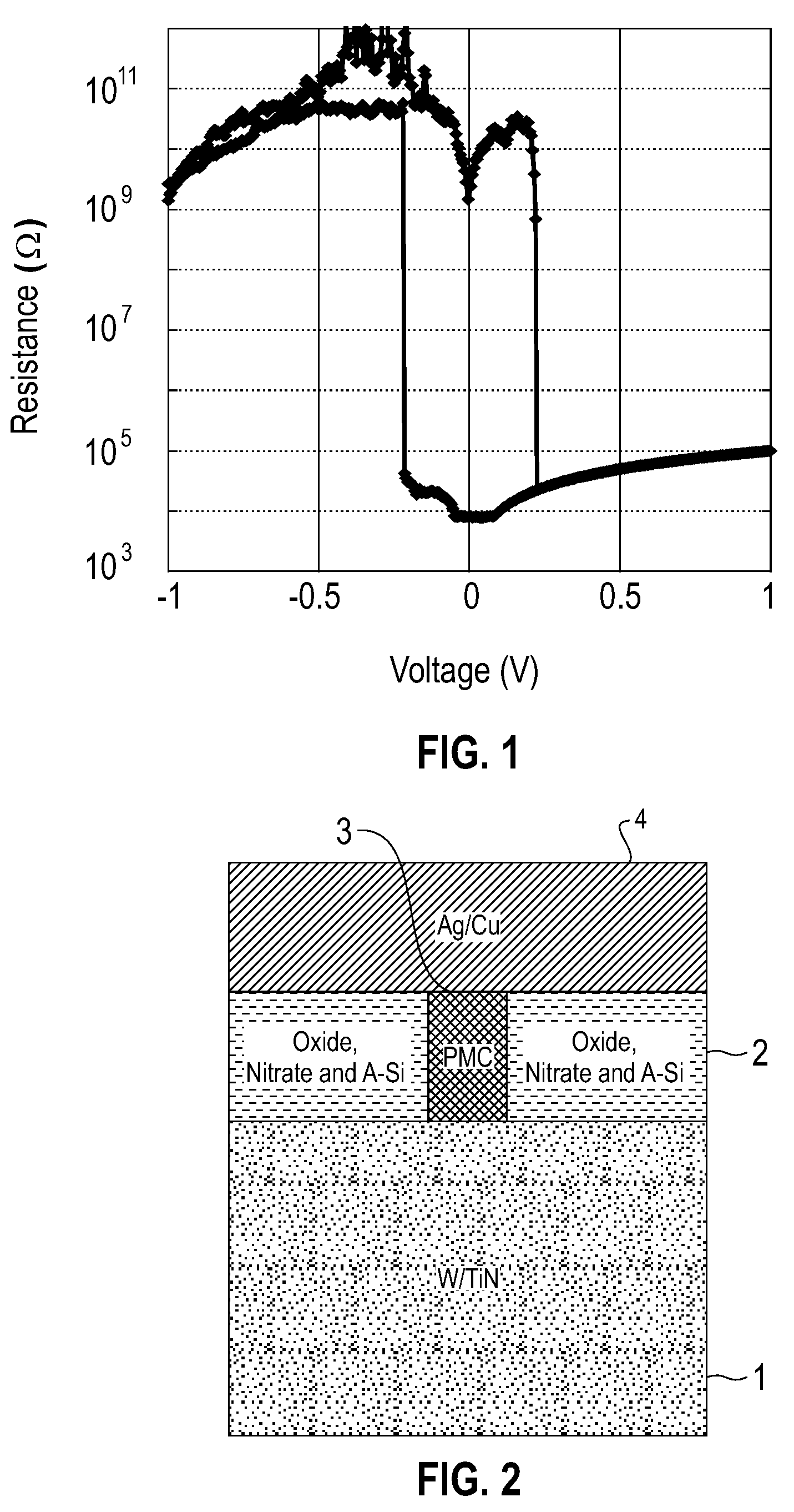
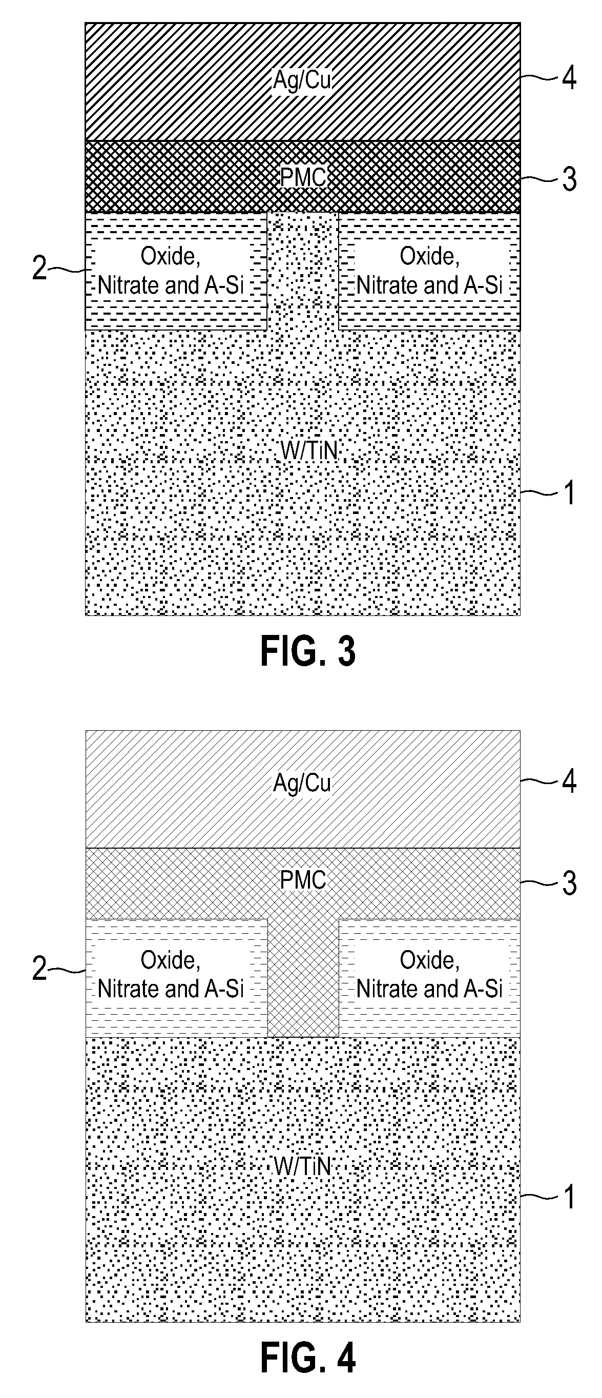
[0071]FIG. 5 illustrates a further embodiment. In this embodiment, the solid electrolyte material 3 is planar and is deposited between 2 layers of metals 1 and 4 (one above and one below that are patterned). The bottom layer consists of the ILD 2 (could be oxide, nitride or low-K material; represented in grey), with imbedded metal 1 (could be W, Cu, TiN, for example; represented in black). The solid electrolyte 3 may or may not be patterned. Ideally, the solid electrolyte 3 is a continuous layer. But patterning may help reduce interference between adjacent cells.
[0075](b) Since a transistor does not exist at every cross-point, also needed is a device that can rectify (exhibit nonlinearity). This ensures that cells that lie on unselected wordlines and bitlines are not inadvertently programmed or shorted to each other.

Problems solved by technology

This results in a very low resistance state (typically <1 Mohm).
A break in the metallic filament can result in high resistance.Typically for times
Such techniques are relatively costly and time-consuming, since they rely on achieving a high-vacuum environment in a confined space prior to the deposition.
In addition, compositional control may be difficult to achieve due to effects such as preferential sputtering in composite targets, the need to balance evaporation rates for multiple evaporation sources and the added difficulty of vacuum-depositing sulfur compounds because of the high vapor pressure of sulfur.
Finally, deposition on complex surfaces (i.e., those containing vias and trenches) can be problematic for directional sputtering techniques.

Method used


Image

  • Electrolytic device based on a solution-processed electrolyte
  • Electrolytic device based on a solution-processed electrolyte
  • Electrolytic device based on a solution-processed electrolyte

Examples


example 1

GeS2 on Si / SiO2

[0081]A film of the GeS2 precursor is readily deposited on a clean thermally-oxidized silicon substrate using a spin-coating technique and the solution described above. Each substrate is pre-cleaned by first using a soap scrub, followed by sequential sonication in ethanol and dichloromethane, and finally using a Piranha clean (hydrogen peroxide: sulfuric acid) with a deionized (DI) water rinse. Thin films of the GeS2 precursor are formed by depositing 2-3 drops of the above-mentioned GeS2 solution onto the substrate, allowing the solution to spread on the substrate for about 10 sec and spinning the substrate at 2000 rpm for about 2 min in a nitrogen-filled drybox.[0082]The resulting precursor films are dried on a hot plate at 100° C. for about 5 minutes in an inert atmosphere, followed by a decomposition heat treatment at 250° C. for about 10 minutes on the same hot plate (gradual heating to this temperature over ½ hr). The latter decomposition heat treatment yields ...

example 2

GeS2 on Ag-Coated Si / SiO2 w / Device Results

[0092]A solution of GeS2 is created by dissolving 0.055 g of GeS2 (0.4 mmol) in 1.6 mL of anhydrous hydrazine (same concentration as in Example 1). The solution is stored about 4 weeks before use for this example. The reaction and resulting solution are maintained in an inert atmosphere (e.g., nitrogen or argon). The solution is filtered through a 0.2 μm syringe filter, while being dispensed onto a substrate for the spin coating process.[0093]A film of the GeS2 precursor is readily deposited onto an Ag-coated (about 200 nm; deposited by e-beam evaporation) p+ silicon substrate using a spin-coating technique and the solution described above. Each Ag-coated substrate is cleaned in an ammonium hydroxide / water mixture for approximately 10 min, rinsed with DI water and blown dry with compressed air before spin coating. Thin films of GeS2 precursor are formed by depositing 2-3 drops of the above-mentioned GeS2 solution onto the substrate, allowing...

example 3

GeS2 Doped with Cu on Si / SiO2

[0098]A solution of GeS2 is created by dissolving 0.055 g of GeS2 (0.4 mmol) in 1.6 mL of the same anhydrous hydrazine as used in Example 2. The solution is stored 24 hr before use. A solution of Cu2S is prepared by stirring 0.159 g of Cu2S (1 mmol) and 0.064 g of S (2 mmol) in 5 mL of anhydrous hydrazine for a period of approximately two weeks. The resulting yellow solution still had a small quantity of black specks, which were removed by filtration through a 0.2 μm syringe filter during dispensing of the solution. The composite solution for spin coating was prepared by stirring (for two minutes) 0.4 mL of the GeS2 solution (containing 0.1 mmol GeS2) with 0.25 mL of the filtered Cu2S solution (containing 0.05 mmol Cu2S). All processing is performed in a nitrogen-filled glove box with oxygen and water levels below 1 ppm.[0099]Each substrate for spin coating was pre-cleaned by first using a soap scrub, followed by sequential sonication in ethanol and dic...


PUM

PropertyMeasurementUnit
Temperatureaaaaaaaaaa

Abstract

The present disclosure relates to a solid electrolyte device comprising an amorphous chalcogenide solid active electrolytic layer; first and second metallic layers. The amorphous chalcogenide solid active electrolytic layer is located between the first and second metallic layers. The amorphous chalcogenide solid active electrolytic layer is prepared by obtaining a solution of a hydrazine-based precursor to a metal chalcogenide; applying the solution onto a substrate; and thereafter annealing the precursor to convert the precursor to the amorphous metal chalcogenide. The present disclosure also relates to processes for fabricating the solid electrolyte device.

Description

CROSS-REFERENCE TO RELATED APPLICATIONS[0001]This application is a continuation of our copending U.S. application Ser. No. 11 / 765,142, filed on Jun. 19, 2007 and entitled “Electrolytic Device and Method of Making Using a Solution-Processed Electrolyte”, entire disclosure of which is incorporated herein by reference.BACKGROUND OF INVENTION[0002]1. Technical Field[0003]The present disclosure relates to an improved electrolytic device. In particular, according to the present disclosure, a high-quality amorphous metal or metalloid chalcogenide film obtained by a relatively high throughput / low-temperature solution-deposition method is used as the active electrolytic layer in the solid-state electrolytic device. The present disclosure also relates to a process for fabricating the solid-state electrolytic device[0004]2. Background Art[0005]In solid-state electrolyte devices, the solid-state electrolyte material generally consists of a Ag-, Cu-, Zn- or Li-doped amorphous chalcogenide (most ...

Claims


Application Information

Patent Timeline
IPC IPC(8): C25B9/06C25B9/17
CPCC23C18/1204H01L45/085H01L45/1233H01L45/141H01L45/142H01L45/1608H01L45/1266H10N70/245H10N70/8416H10N70/8822H10N70/882H10N70/021H10N70/826C23C18/12H10N70/00
Inventor GOPALAKRISHNAN, KAILASHMITZI, DAVID B.SHENOY, ROHIT S.
Owner GLOBALFOUNDRIES INC
Learn More