Junction Termination Extension with Controllable Doping Profile and Controllable Width for High-Voltage Electronic Devices

a technology of junction termination and controllable width, applied in the field of semiconductor devices, can solve the problems of time and money, the dopant does not diffuse effectively in silicon, and the dopant island-implantation technique that provides a smooth graded junction termination doping profile in silicon does not work well

Active Publication Date: 2010-03-04
THE UNITED STATES OF AMERICA AS REPRESENTED BY THE SECRETARY OF THE NAVY
View PDF7 Cites 51 Cited by
  • Summary
  • Abstract
  • Description
  • Claims
  • Application Information

AI Technical Summary

Benefits of technology

[0010]This summary is intended to introduce, in simplified form, a selection of concepts that are further described in the Detailed Description. This summary is not intended to identify key or essential features of the...

Problems solved by technology

However, dopants do not diffuse effectively in silicon carbide, and thus the dopant island-implantation technique that provides a smoothly graded junction termination doping profile in silicon does not work well.
Both of these methods for producing graded junction termination extensions can result in excellent parallel-plate breakdown voltage, but both also have significant drawbacks.
However, fabrication of a graded junction termination extension using this method requires multiple doping steps, and therefore can be expensive, both in terms of time and money.
In addition, each transition between the stepped regions is a potential breakdown point due to differences in doping levels and differences in voltage in each zone, and at high voltages (i.e., higher than 2.4 kV), these differences can result in a complete break...

Method used


Image

  • Junction Termination Extension with Controllable Doping Profile and Controllable Width for High-Voltage Electronic Devices
  • Junction Termination Extension with Controllable Doping Profile and Controllable Width for High-Voltage Electronic Devices
  • Junction Termination Extension with Controllable Doping Profile and Controllable Width for High-Voltage Electronic Devices

Examples


example 1

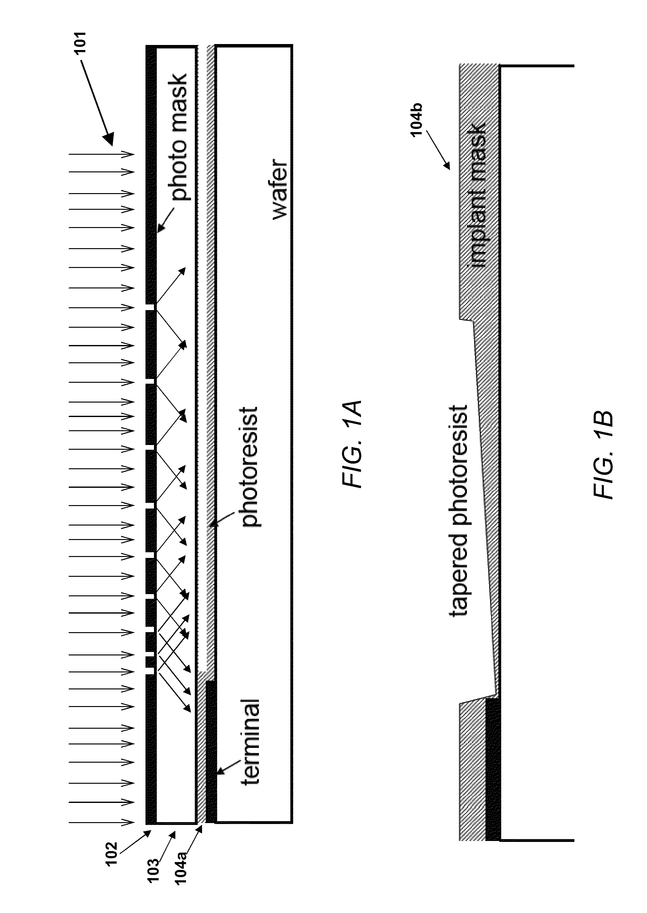
[0037]1. Use a specially designed mask, separated from the photoresist by a controlled gap or clear spacer, to produce a laterally tapered photoresist layer having controlled arbitrary lateral thickness profile and a controlled arbitrary lateral width on the semiconductor substrate in the junction termination extension region surrounding the high voltage junction.

[0038]2. Develop and bake the photoresist, using any conventional methods for developing a photoresist, such as immersion in a commercially available development solution for a time on the order of 1 minute followed by baking with a 120 degree Celsius oven or hotplate.

[0039]3. Optionally convert the photoresist to graphite (or carbon) by heating at approximately greater than 500 C in a nitrogen or argon ambient. The resist will flow and smooth out to some degree during the heating.

[0040]4. Perform a dopant ion implantation (for example, P-type dopant such as boron or aluminum) at a selected ion implant energy and dose into ...

example 2

[0045]1. Form a dopant layer in a semiconductor.

[0046]2. Use a specially designed mask, separated from the photoresist by a controlled gap or clear spacer, to produce a laterally tapered photoresist layer having a controlled arbitrary lateral thickness profile and a controlled arbitrary lateral width on the semiconductor substrate in the junction termination extension region surrounding the high voltage junction.

[0047]3. Develop and bake the photoresist.

[0048]4. Optionally convert the photoresist to graphite (or carbon) by heating at approximately greater than 500 C in a nitrogen or argon ambient. The resist will flow and smooth out to some degree during the heating.

[0049]5. Use an RIE etcher to simultaneously etch laterally tapered material (for example, photoresist) and the semiconductor material. Typically, the etch rate of the laterally tapered material and the semiconductor material will be at different rates, but for optimized etch gases, RF power, and pressure in the RIE, nea...

example

[0067]Creation of a junction termination extension having a controlled arbitrary lateral doping profile and a controlled arbitrary lateral width using a gray-scale lithography technique and tapered implantation mask having one or more features described herein is now described in the context of the following example.

[0068]The lithography technique and implantation mask were implemented in all-implanted silicon carbide pn junction diodes. The starting material was 38 μm of n-doped (7×1014 cm−3) epitaxy grown on top of an n+ buffer layer on an 8° off-axis 4H—SiC substrate. After creating alignment features with reactive ion etching, a thick layer of positive photoresist was spin-deposited on the wafer.

[0069]The tapered implantation mask was formed using a grayscale lithography technique. Grayscale exposure was accomplished by using a two-tone sub-resolution mask. In this exemplary implementation, the mask had circular diode anode openings that were 100 μm in diameter. Around the anode...


PUM


Abstract

Methods for producing a junction termination extension surrounding the edge of a cathode or anode junction in a semiconductor substrate, where the junction termination extension has a controlled arbitrary lateral doping profile and a controlled arbitrary lateral width, are provided. A photosensitive material is illuminated through a photomask having a pattern of opaque and clear spaces therein, the photomask being separated from the photosensitive material so that the light diffuses before striking the photosensitive material. After processing, the photosensitive material so exposed produces a laterally tapered implant mask. Dopants are introduced into the semiconductor material and follow a shape of the laterally tapered implant mask to create a controlled arbitrary lateral doping profile and a controlled lateral width in the junction termination extension in the semiconductor.

Description

CROSS-REFERENCE[0001]This application claims the benefit of priority based on U.S. Provisional Patent Application No. 61 / 093,738 filed on Sep. 3, 2008, the entirety of which is hereby incorporated by reference into the present application.TECHNICAL FIELD[0002]The present invention relates to semiconductor devices and semiconductor fabrication processes for high voltage applications.BACKGROUND[0003]Planar high-voltage semiconductor rectifier and switching devices typically require edge termination around the high-voltage terminal pn junction. In general the goal is to produce a smoothly tapered field profile to prevent high-voltage field-crowding that causes premature breakdown at the edge of the high voltage electrode. Without such a termination, the regions of high field curvature around the edges of the terminal reach the fundamental breakdown voltage far below the parallel plane limit. Such premature breakdown can be reduced somewhat by means of a field-plate or single-zone junct...

Claims


Application Information

Patent Timeline
IPC IPC(8): H01L21/20H01L21/265
CPCH01L21/0465H01L29/0615H01L29/868H01L29/6606H01L29/8611H01L29/1608H01L21/0274H01L21/3085
Inventor IMHOFF, EUGENE A.KUB, FRANCIS J.HOBART, KARL D.
Owner THE UNITED STATES OF AMERICA AS REPRESENTED BY THE SECRETARY OF THE NAVY
Why Eureka
Try Eureka