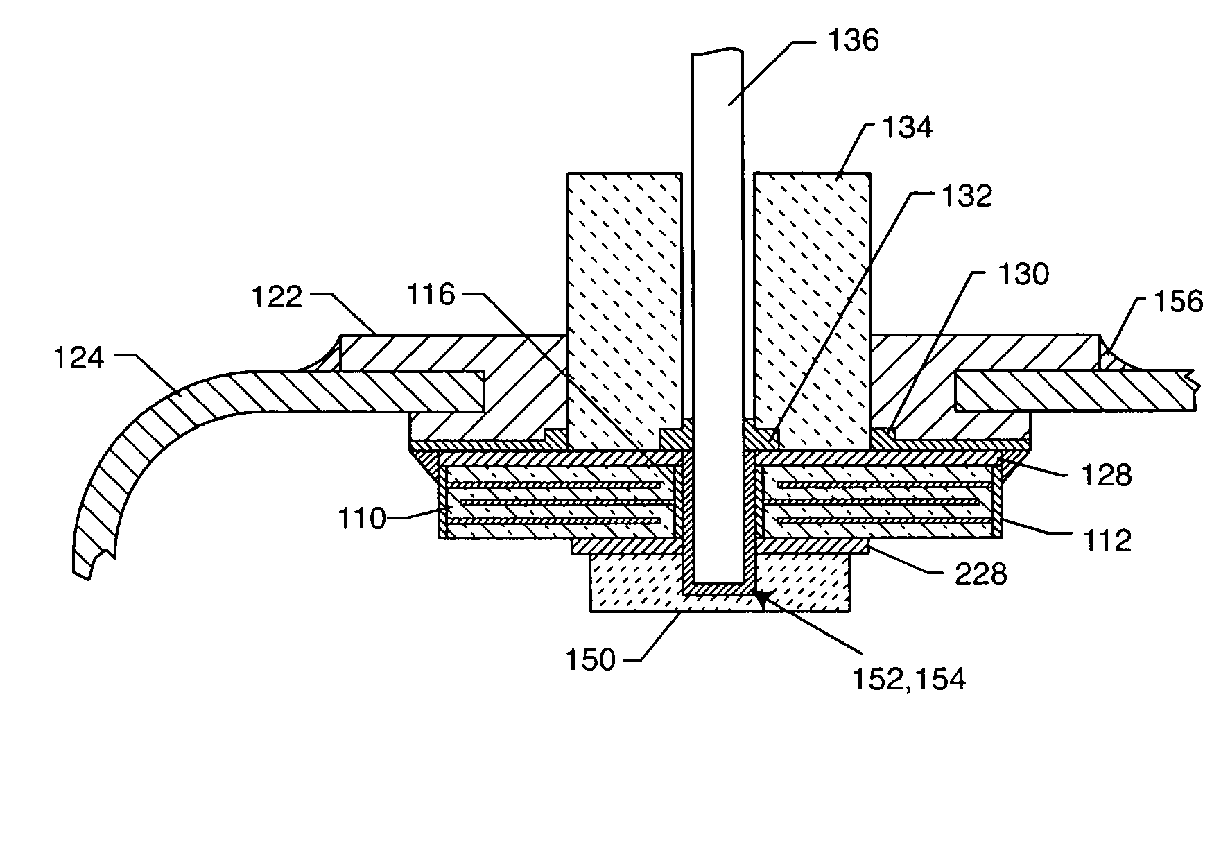
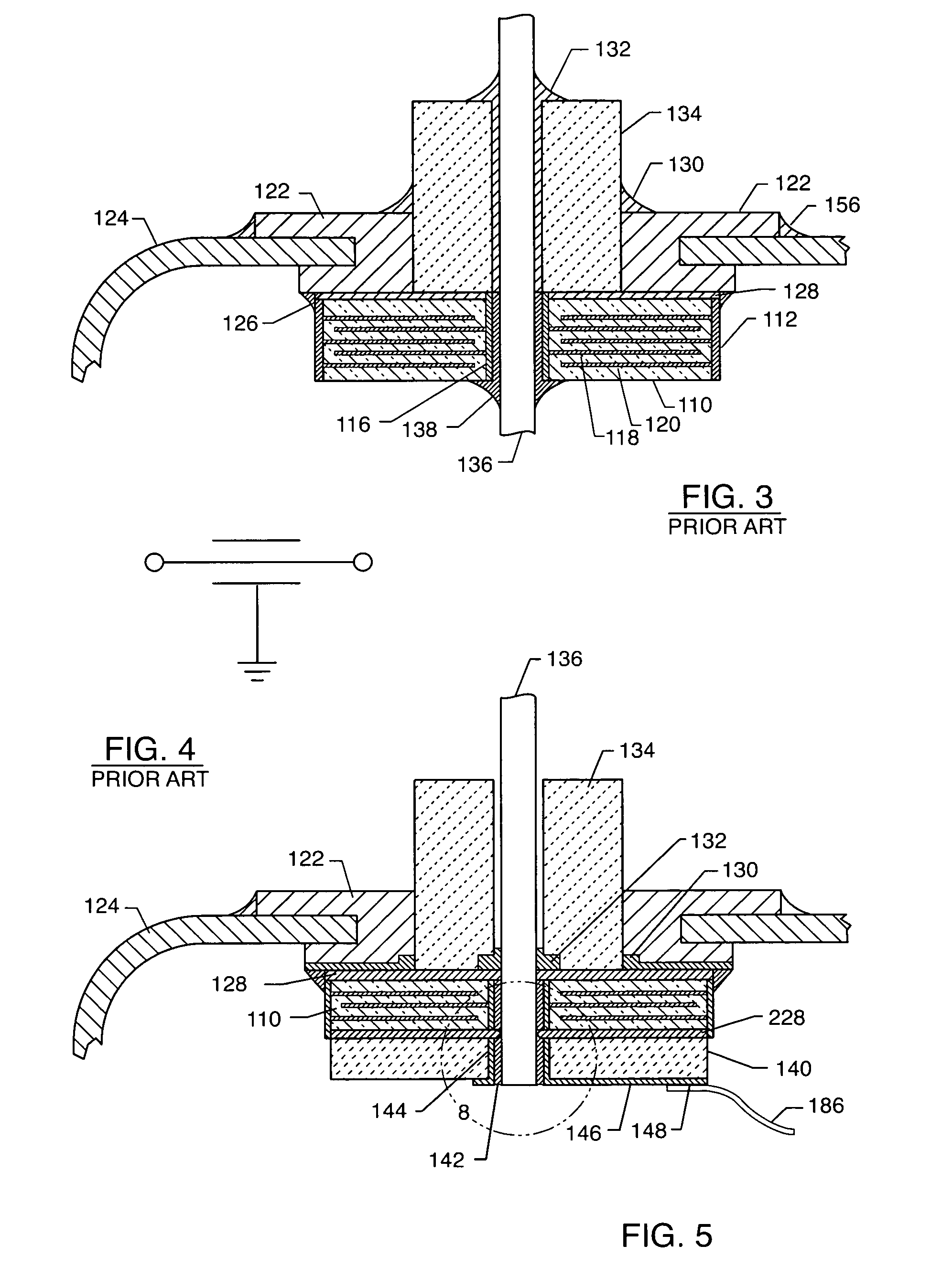
[0008] In a preferred embodiment, a substrate or circuit board having attached wire bond pads is co-bonded to the
ceramic capacitor in such a way that they act as a monolithic structure. The co-bonded circuit board or substrate contains via holes, circuit traces and bonding pads or bonding areas such that it is convenient to attach wires from the circuitry inside the implantable
medical device to the
feedthrough capacitor structure via thermosonic bonding,
ultrasonic bonding, thermal-setting conductive adhesives,
soldering,
welding,
brazing, mechanical attachments or the like. In a preferred embodiment, a novel circuit board or substrate is co-bonded to the top surface of the
ceramic feedthrough capacitor in accordance with the invention. The co-bonding is performed with a
thin layer of high temperature thermal setting material such as a nonconductive
polyimide. Ideal material for this application is a thermal plastic
polyimide supported tape
adhesive whose properties are described herein in FIG. 6. There are a number of alternate materials that can be used to co-bond the circuit board or substrate to the surface of the
ceramic capacitor including various nonconductive thermal-setting polymers such as high temperature thermal setting epoxies, silicones, polyimides, adhesives, sealants and the like. Another method of co-bonding could include co-firing with low temperature glasses, ceramics or the like. The substrate or circuit board can be made of a number of materials that are common in the art. For the present application, an ideal
ceramic substrate material would include, but are not limited to the group of: Aluminum-
oxide, Fosterite,
Alumina in various purities, Berrylia and Aluminum
Nitride. These ceramic substrates are well known in the art, have good mechanical or
laser scribe characteristics and do not greatly mismatch the
thermal coefficient of expansion of the
ceramic capacitor and therefore will prevent the formation of excessive mechanical stresses that could fracture the
ceramic capacitor. For ceramic substrates, the scribe characteristics of the ceramic material is important so that the individual substrates of the present invention can be
cut or snapped out of the larger production array of such substrates.
[0011] Accordingly, one can see from the above listing, that polyimides, followed by
cyanate esters and BT epoxies would be a preferred choice after ceramic substrates as an alternative for the present invention. As used herein, the word substrate or
alumina substrate can include any of the ceramic or non-
ceramic materials listed above, in addition to many others that are not shown. It is desirable that the material that bonds the substrate of the circuit board to the
ceramic capacitor be somewhat flexible and stress absorbing. This flexible layer will help prevent
cracking of the ceramic capacitor due to any mismatches in the thermal coefficients of expansion. Accordingly,
polyimide is an ideal material in that it forms a
ring type of molecule after it goes through its
glass transition temperature of approximately 260° C. Compared to
epoxy, this material tends to absorb stresses and is quite resilient.
[0012] A novel aspect of the present invention is that both the ceramic
feedthrough capacitor(s) and the circuit board or substrate can be made much thinner than conventional practice because they are co-bonded into a monolithic laminate structure. This co-bonded / laminated structure is analogous to a beam. By increasing the height of the beam one dramatically increases the
moment of inertia of the beam. A beam with an increased
moment of inertia is much more resistant to failure or
cracking due to bending forces. For example, if there was a
bending force which tended to deflect the
composite structure in a downward fashion, the top of the capacitor would be in compression and the bottom would tend to be in tension. By raising the
moment of inertia of this
composite structure, the amount of deflection is minimized. Accordingly, a novel aspect of the present invention is that a circuit board or substrate can be added without greatly increasing the overall volume (height) of the EMI filter.
[0016] It should be noted that if lead-attachment is made by
soldering or the like, the
Kovar or
Alloy 42 pad is generally not required. However, during ultrasonic or thermal
wire bonding, considerable energy is imparted into the structure. Accordingly, in this case, a
Kovar pad is desired to dissipate energy away from the underlying
ceramic substrate or feedthrough capacitor structure. When
wire bonding using thermosonic or ultrasonic energy, it is desirable to also use an
alumina substrate which is co-bonded to the ceramic capacitor. This
alumina substrate, when it is co-bonded, distributes the
wire bonding shock and vibration forces across the entire surface of the ceramic capacitor. In general,
ceramic materials, and capacitor dielectrics in particular, are strong in compression but very weak in tension. The relatively strong co-bonded alumina substrate helps protect the relatively weak
barium titanate,
strontium titanate or equivalent high K
dielectric used in the ceramic capacitor from fracturing or forming micro-cracks during application of these wire bonding forces. As a general rule, as one raises the
dielectric constant, K, of a ceramic material, the structurally weaker it becomes. A low K alumina or aluminum
oxide substrate is generally much stronger than
barium titanate or other high K ceramics and is able to withstand these wire bonding forces. In this way, tension, shear and
impact forces do not build up or become excessive in the capacitor
dielectric. Various substrates are well known in the art with wire bond pads and are typically used in combination with
hybrid circuit electrical connections and the like.


