Method for optimizing passivation of gallium nitride high-electron-mobility transistor
A high electron mobility, transistor technology, applied in circuits, electrical components, semiconductor devices, etc., can solve problems such as device performance, stability degradation, gallium nitride material surface damage, current collapse, etc., to reduce current collapse and reduce Effects of Interface Defects and Gate Leakage Reduction
- Summary
- Abstract
- Description
- Claims
- Application Information
AI Technical Summary
Problems solved by technology
Method used
Image

Examples
Embodiment 1
[0035] A method for optimizing the passivation of GaN high electron mobility transistors includes:
[0036] First, use MOCVD equipment to sequentially grow a GaN channel layer, an AlGaN barrier layer, and a GaN capping layer on a silicon, sapphire, or silicon carbide substrate to form a GaN / AlGaN / GaN structure sample;
[0037] Second, the mesa of the active region is etched on the sample of the GaN / AlGaN / GaN structure, and the alloy electrodes of the source and drain regions are prepared on the mesa of the active region by electron beam evaporation, and the source and drain are at 700°C~900°C Perform rapid annealing in a nitrogen atmosphere at ℃ for 30s~60s to form an ohmic contact;
[0038] Third, place the sample after forming the source and drain electrodes in an acid solution with a concentration of 1% to 20% for 1 minute to 20 minutes to remove the natural oxide layer on the sample,
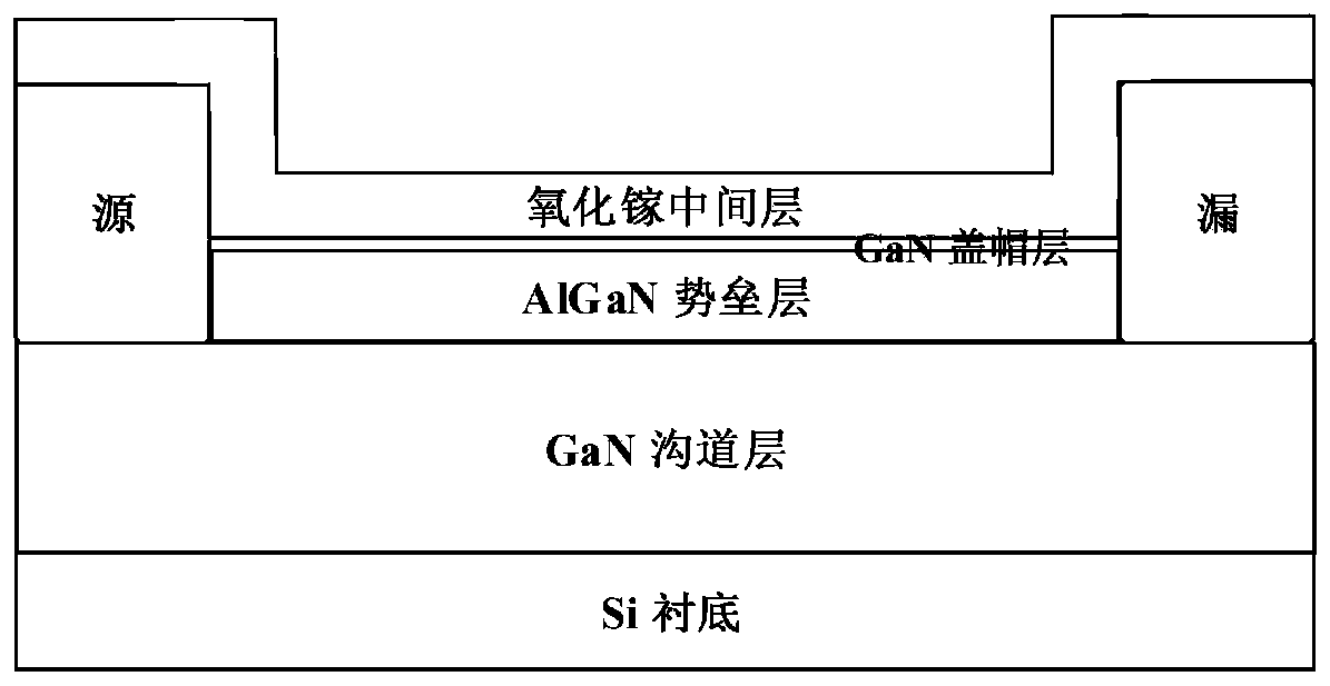
[0039] Fourth, after removing the natural oxide layer, put the sample into the ALD or P...
Embodiment 2
[0046] A method for optimizing the passivation of gallium nitride high electron mobility transistors, the steps are as follows:
[0047] 1. Use MOCVD to sequentially grow a GaN channel layer with a thickness of 0~6000nm, an AlGaN barrier layer with a thickness of 0~50nm, and a GaN cap layer with a thickness of 0~10nm on the substrate.
[0048] 2. On the GaN / AlGaN / GaN sample with the above structure, the active region mesa is formed by photolithography and ICP etching technology, and the ICP etching depth is 1~1000nm.
[0049] 3. Prepare source and drain alloy electrodes by electron beam evaporation of source and drain electrode materials, and perform rapid thermal annealing in a nitrogen atmosphere to form ohmic contacts.
[0050] 4. After the ohmic contact is formed, soak the sample in hydrochloric acid solution at room temperature to remove the natural oxide layer on the surface; rinse with deionized water after completion, and blow dry with nitrogen.
[0051]5. Put the sam...
Embodiment 3
[0058] as attached Figure 1-6 As shown, a method for optimizing the passivation of GaN high electron mobility transistors, the steps include:
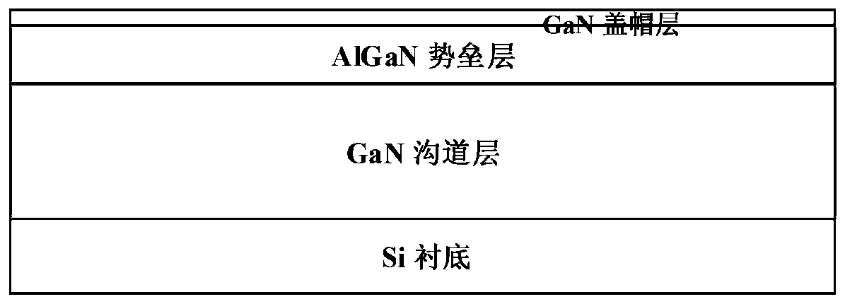
[0059] (1) if figure 1 As shown, on the Si substrate, a GaN channel layer is first grown by MOCVD, a layer of AlGaN barrier layer of about 25nm is grown on it, and finally a GaN surface cap layer is grown.
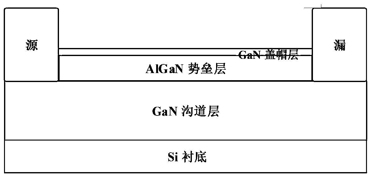
[0060] (2) On the gallium nitride heterojunction substrate with the above structure, a mesa with a high active region of about 300nm is formed by photolithography and ICP etching technology.
[0061] (3) Photolithography is carried out on the prepared active area, and the source and drain electrode areas are photolithographically etched, and the four materials of Ti / Al / Ni / TiN (30nm / 120nm / 60nm / 60nm) are evaporated by electron beams, and prepared by lift-off process Metal electrodes for the source and drain regions. And perform rapid annealing in a nitrogen atmosphere at 860 °C for 40 seconds to form an ohmic contact, the cross-s...
PUM
| Property | Measurement | Unit |
|---|---|---|
| thickness | aaaaa | aaaaa |
| thickness | aaaaa | aaaaa |
| thickness | aaaaa | aaaaa |
Abstract
Description
Claims
Application Information
 - R&D
- Intellectual Property
- Life Sciences
- Materials
- Tech Scout
- Unparalleled Data Quality
- Higher Quality Content
- 60% Fewer Hallucinations
Browse by: Latest US Patents, China's latest patents, Technical Efficacy Thesaurus, Application Domain, Technology Topic, Popular Technical Reports.
© 2025 PatSnap. All rights reserved.Legal|Privacy policy|Modern Slavery Act Transparency Statement|Sitemap|About US| Contact US: help@patsnap.com