


Quick Research
Generate reliable direction feasibility study reports for your R&D in just a few steps.

Technical Q&A
Discover and master advanced knowledge NOW. Basics, ideas, possibilities, all at once.

Find Solutions
As an expert in R&D theories, this can generate solutions to your technical problems instantly.

Evaluate Feasibility
Analyze your overall solution with one click, know your potential R&D risks in advance.

Monitor Landscape
Get weekly tech updates, stay abreast of the latest tech innovations and key insights.
Preparation method of composite mask for high-energy ion implantation
A composite mask and high-energy ion technology, which is applied in semiconductor/solid-state device manufacturing, electrical components, circuits, etc., can solve the problem that photoresist masks are easy to remain, there are many process errors in graphic dimensions, and the blocking effect of thin film masks is affected and other problems, to avoid device process failure, avoid mask residues, and shorten the glue removal time
- Summary
- Abstract
- Description
- Claims
- Application Information
AI Technical Summary
Problems solved by technology
Method used
Image

Examples
Embodiment 1
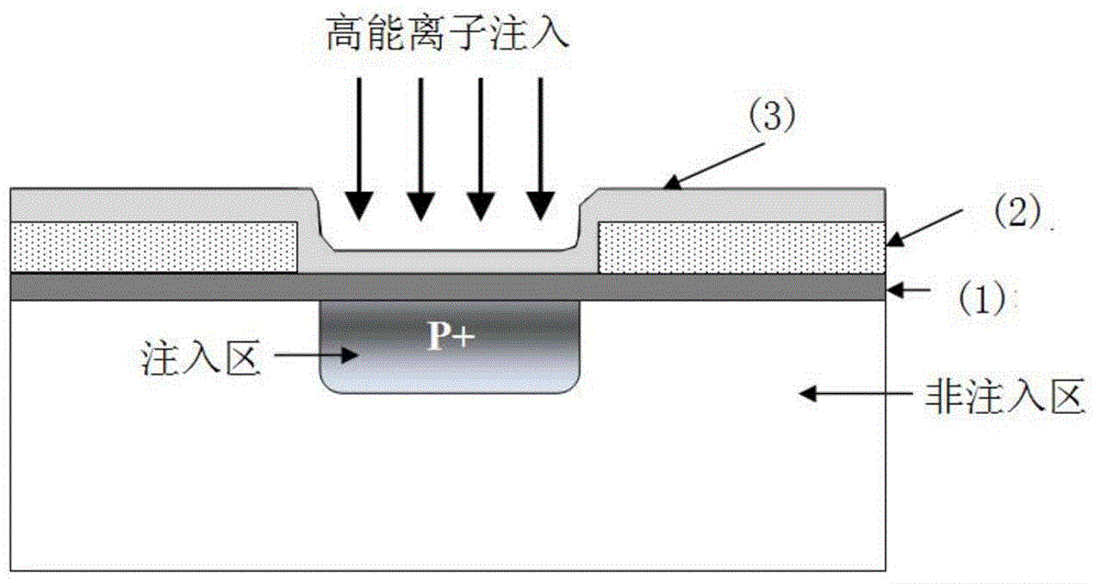
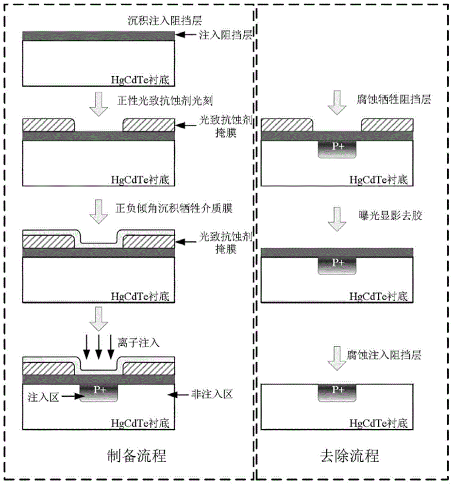
[0025] Using the mask preparation method described in the present invention, evaporation deposition, photolithography and positive and negative tilt angle evaporation deposition are performed on the surface of the mercury cadmium telluride epitaxial material chip. The preparation process is as attached figure 2 Shown. First, after annealing and surface corrosion treatment, the surface of the HgCdTe epitaxial material chip is thermally evaporated to deposit a 60nm thick cadmium telluride injection barrier layer, the chip is cleaned, and a layer of 2 to 3 microns is spin-coated on the chip surface A thick positive photoresist is used to expose the chip to ultraviolet light with a photolithography plate. After development and fixation, a photoresist injection mask is obtained.
[0026] Load the chip with the prepared mask pattern on the sample stage of the high-vacuum thermal evaporation equipment, first rotate the sample stage at an inclination angle of 0° to deposit a ~20nm thick ...
Embodiment 2
[0030] Using the mask preparation method described in the present invention, evaporation deposition, photolithography and positive and negative tilt sputtering deposition are performed on the surface of the mercury cadmium telluride epitaxial material chip. The preparation process is as attached figure 2 Shown. First, after annealing and surface corrosion treatment, a -20nm thick cadmium telluride injection barrier layer is thermally evaporated on the surface of the HgCdTe epitaxial material chip after the annealing treatment and surface corrosion treatment, the chip is cleaned, and a layer of 2 to 3 microns is spin-coated on the chip surface A thick positive photoresist is used to expose the chip to ultraviolet light with a photolithography plate. After development and fixation, a photoresist injection mask is obtained.
[0031] Load the chip with the mask pattern prepared on the sample stage of the magnetron sputtering equipment. First, rotate the sample stage at an inclination...
Embodiment 3
[0035] Using the mask preparation method described in the present invention, evaporation deposition, photolithography and positive and negative tilt angle evaporation deposition are performed on the surface of the mercury cadmium telluride epitaxial material chip. The preparation process is as attached figure 2 Shown. First, after annealing and surface corrosion treatment, the surface of the mercury cadmium telluride epitaxial material chip is thermally evaporated to deposit a ~200nm thick cadmium telluride injection barrier layer, the chip is cleaned, and the chip surface is spin-coated with a thickness of 2 to 3 microns A thick positive photoresist is used to expose the chip to ultraviolet light with a photolithography plate. After development and fixation, a photoresist injection mask is obtained.
[0036] Load the chip with the prepared mask pattern on the sample stage of the high-vacuum thermal evaporation equipment. First, rotate the sample stage at an inclination angle of ...
PUM
| Property | Measurement | Unit |
|---|---|---|
| thickness | aaaaa | aaaaa |
Abstract
Description
Claims
Application Information
 - R&D Engineer
- R&D Manager
- IP Professional
- Industry Leading Data Capabilities
- Powerful AI technology
- Patent DNA Extraction
Browse by: Latest US Patents, China's latest patents, Technical Efficacy Thesaurus, Application Domain, Technology Topic, Popular Technical Reports.
© 2024 PatSnap. All rights reserved.Legal|Privacy policy|Modern Slavery Act Transparency Statement|Sitemap|About US| Contact US: help@patsnap.com