Preparation method of nano zinc oxide thin film and zinc oxide/copper oxide semiconductor material
A nano-zinc oxide and semiconductor technology, which is applied in semiconductor/solid-state device manufacturing, semiconductor devices, metal material coating technology, etc., can solve environmental pollution and other problems, and achieve the effects of low preparation cost, easy control of technical parameters, and simple equipment
- Summary
- Abstract
- Description
- Claims
- Application Information
AI Technical Summary
Problems solved by technology
Method used
Image
Examples
Embodiment 1
[0023] The present embodiment is the preparation method of nano zinc oxide thin film, and its specific steps are as follows:
[0024] 1) Use semi-automatic amorphous strip preparation equipment to continuously spray liquid zinc onto the wall of a high-speed rotating copper cylinder to rapidly cool it to form a metal zinc strip with a thickness of 40 μm;
[0025] 2) Put the metal zinc strip into a beaker, add absolute alcohol, ultrasonically clean it for 15 minutes, then rinse it with distilled water, dry it, and put the cleaned metal zinc strip into a 1mol / L copper sulfate solution at room temperature for erosion for 3 seconds, the surface of the metal zinc strip turns black, take out the metal zinc strip, dry naturally, and place the metal zinc strip in the crucible;
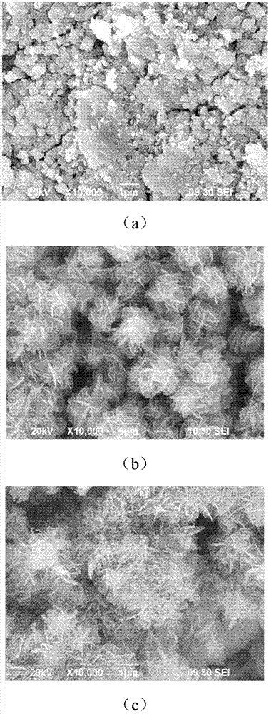
[0026] 3) After the temperature in the tube furnace rises to 350°C, 400°C, 500°C, 550°C and 600°C respectively, put the metal zinc strip and the crucible into the furnace, keep it warm in the air for 3 hours, a...
Embodiment 2
[0031] This embodiment is a preparation method of zinc oxide / copper oxide semiconductor material, and its specific steps are as follows:
[0032] 1) Put the metal zinc strip in Example 1 into a beaker filled with absolute alcohol, ultrasonically clean it for 15 minutes, rinse it with distilled water, dry it, and put the cleaned metal zinc strip into sulfuric acid with a concentration of 1mol / L In the copper solution for 3 seconds, take out the metal zinc strip to dry naturally, and place the metal zinc strip in the crucible;
[0033] 2) After the temperature in the tube furnace rises to 700°C, put the metal zinc strip and the crucible into the furnace, keep it warm in the air for 3 hours, and cool it down to room temperature naturally to obtain zinc oxide / oxide with zinc as the base material. copper semiconductor material.
[0034] The zinc oxide / copper oxide semiconductor material prepared in this embodiment is used as a sample to carry out the following tests:
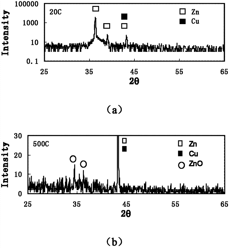
[0035] The...
Embodiment 3
[0038] The present embodiment is the preparation method of nano zinc oxide thin film, and its specific steps are as follows:
[0039]1) Use 1000# water abrasive paper to grind the surface of industrial pure zinc sheet with a thickness of 0.3mm to remove the oxide film on the surface, put the polished zinc sheet into a beaker, clean it ultrasonically with acetone for 10 minutes, and then ultrasonically clean it with distilled water for 10 minutes. Finally, rinse with absolute alcohol and let it dry naturally;
[0040] 2) Immerse the cleaned zinc flakes in 1mol / L copper sulfate solution for 5 seconds, the surface of the zinc flakes will turn black, take them out, and put them into a boat-shaped crucible after the zinc flakes are naturally dried;
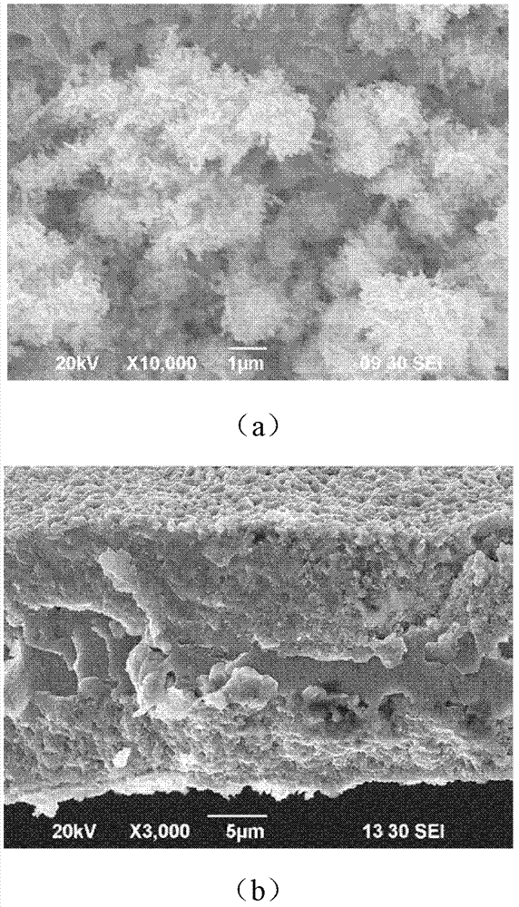
[0041] 3) Raise the temperature in the tubular resistance furnace to 500°C, and feed different proportions of nitrogen and oxygen into the furnace at the same time to obtain different partial pressures of oxygen (~0.001%, 5%, 15%, 25%,...
PUM
| Property | Measurement | Unit |
|---|---|---|
| thickness | aaaaa | aaaaa |
Abstract
Description
Claims
Application Information
 - R&D
- Intellectual Property
- Life Sciences
- Materials
- Tech Scout
- Unparalleled Data Quality
- Higher Quality Content
- 60% Fewer Hallucinations
Browse by: Latest US Patents, China's latest patents, Technical Efficacy Thesaurus, Application Domain, Technology Topic, Popular Technical Reports.
© 2025 PatSnap. All rights reserved.Legal|Privacy policy|Modern Slavery Act Transparency Statement|Sitemap|About US| Contact US: help@patsnap.com


