Thin film photovoltaic structure

Inactive Publication Date: 2007-12-06
CORNING INC
View PDF35 Cites 187 Cited by
  • Summary
  • Abstract
  • Description
  • Claims
  • Application Information

AI Technical Summary

Benefits of technology

[0074]The advantages of this invention are best understood after reading the detailed technical description, and in relation to existing SOI processes. Nonetheless, the primary advantages include: photovoltaic structure variation; thinner silicon films; more uniform silicon films with higher crystal quality; faster manufacturing throughput; improved manufacturing yield; reduced contamination; and scalability to large substrates. These benefits naturally combine to reduce costs.
[0078]As demand continues to rise, faster throughput is critical. However, the polishing technologies identified for fabricating SiOG have process times on the order of tens of minutes, and the furnace anneals can be several hours. With more uniform films, the need in photovoltaic cells for polishing or furnace annealing is reduced.
[0079]Improving manufacturing yield is also important for waste and cost reduction. By avoiding the wire-saw kerf loss, material waste may be reduced significantly. Likewise, the expensive donor semiconductor wafer may be polished and reused multiple times. By using thin films, material consumption likewise may be reduced significantly. If polishing of the SOI structure is avoided, the overall manufacturing yield is expected to improve. This is particularly true if the polishing process has a low step yield, as anticipated. The process window is expected to be large because of the crystalline nature of the film, and therefore the yield is expected to be high.
[0080]Due to the sensitive nature of SOIs, contamination adversely may affect performance, so reducing contamination is highly desirable. With this in mind, avoiding the need for polishing with an abrasive slurry to reduce layer thickness reduces the potential for contamination. Furthermore, avoiding the need for a furnace anneal also avoids the diffusion of contaminants that may occur during a lengthy thermal anneal process. This may play an important consideration in the efficiency of the photovoltaic devices.
[0081]The process is scalable to large areas. This scalability potentially extends the product life as customer substrate size requirements increase. Solar panels are often large to maximize use of available space, so the larger photovoltaic cells become, the fewer photovoltaic cells are necessary to connect to create a large solar panel. In contrast, surface polishing and furnace annealing become increasing difficult for larger substrate sizes.
[0082]In particular, key advantages of preferred embodiments of the present invention include: 1) the use of low cost, expansion-matched glass or glass ceramic substrates, compared to other more expensive semiconductor substrates (such as silicon for a Ge layer and subsequent GaAs growth, as has been used previously) or thermally mismatched ceramic substrates described in the prior art; 2) the presence of the single crystal template layer of Si, Ge or multilayer GaAs / Ge on the glass substrate, which is used as a template to create lattice matched, very low defect semiconductor layers for the solar cells with high efficiencies, unlike polycrystalline templates used in prior art; 3) the transparency of the substrate allowing flexibility in module fabrication.

Problems solved by technology

The primary issues with the use of bulk Si are the cost and supply of so-called solar grade silicon and its utilization.
With a typical bulk crystal-Si or p-Si solar cell of 200 microns thick, the kerf loss from cutting wafers from boules or cast ingots is approximately 30%, significantly contributing to the overall cost.
Single crystalline wafers which are used in the semiconductor industry can be made in to excellent high efficiency solar cells, but they are generally considered to be too expensive for large-scale mass production.
Thin-film solar cells use less than 1% of the raw material (silicon or other light absorbers) compared to wafer based solar cells, leading to a significant price drop per kWh.
This can lead to reduced processing costs from that of bulk materials (in the case of silicon thin films) but also tends to reduce energy conversion efficiency, although many multi-layer thin films have efficiencies above those of bulk silicon wafers.
For a-Si, efficiency of energy conversion is a major issue, with a common range of 10%-13%.
They are also some of the most expensive cells per unit area.
Defects in the crystal structure of the semiconductor can impede performance considerably.
Though, the highest efficiency cells often are not the most economical—for example a 30% efficient multijunction cell based on exotic materials such as gallium arsenide or indium selenide and produced in low volume might well cost one hundred times as much as an 8% efficient amorphous silicon cell in mass production, while only delivering a little under four times the electrical power.
Thin film Si PVS technology also has issues, inasmuch as the process temperatures used in the literature are near the melting point of Si, so there are considerable constraints on the substrate (purity, expansion coefficient, ability to contact the cell, etc.).
Cost is an issue for CIGS PVS, made of multi-layered thin-film composites.
Manufacturability is an issue for both CIS and CdTe PVS, which have difficulties achieving uniformity of performance over large areas.
While CIS films can achieve 11% efficiency, their manufacturing costs are high at present.
However, Cd is regarded as a toxic heavy metal, reducing the incentive for development.
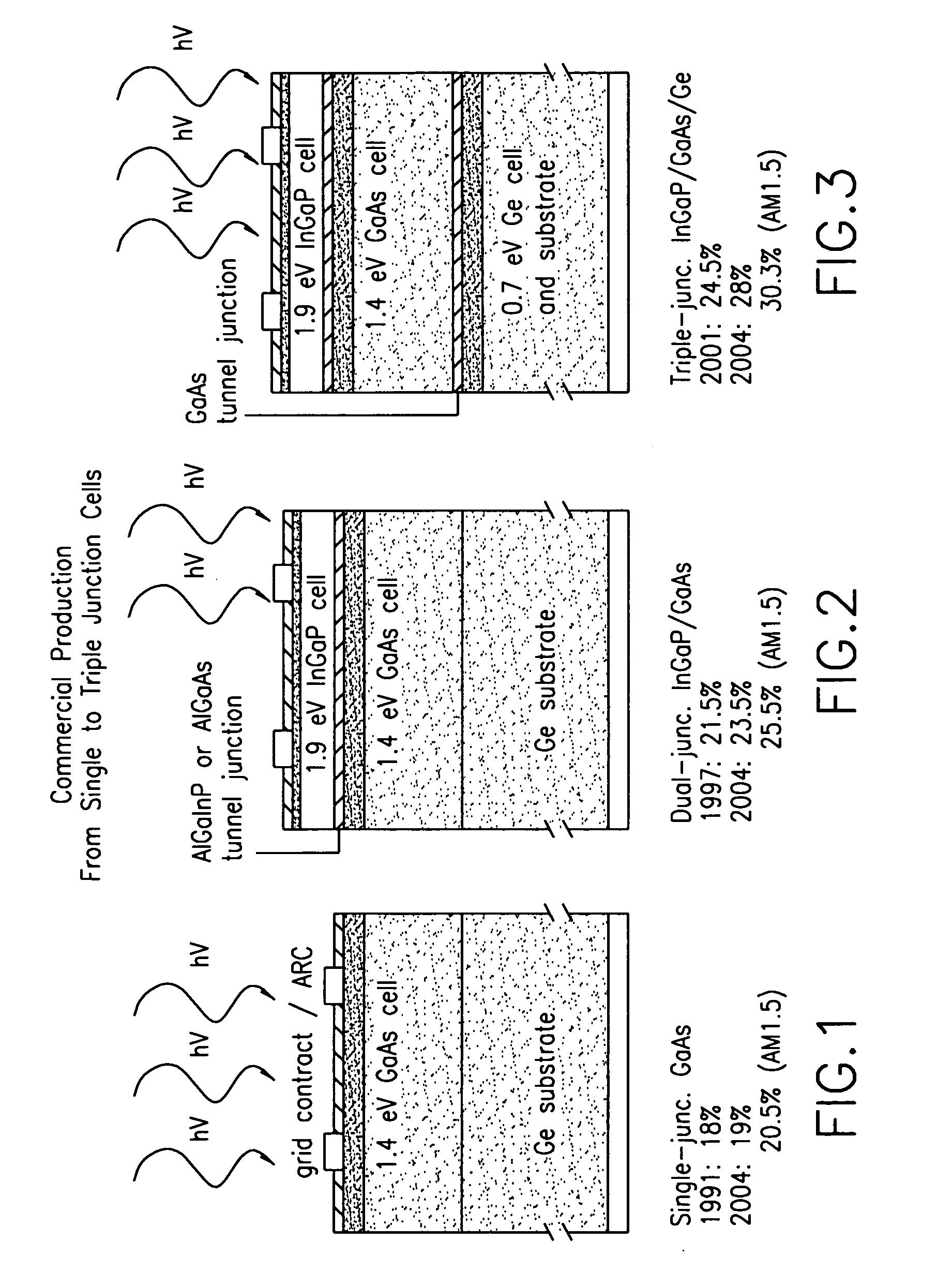
Cost also is an issue for high-efficiency gallium arsenide (GaAs) multijunction cells, which have been developed for special applications such as satellites and space exploration that require high-performance.
Factoring into the cost is the formation of ohmic contacts, discussed more below, to such compound semiconductors, which is considerably more difficult than with silicon.
In addition, the volatility of As limits the amount of post-deposition annealing that GaAs devices will tolerate.
Contacts are often made by first depositing the transition metal and second forming the silicide by annealing, with the result that the silicide may be non-stoichiometric.
Tempered glass typically is incompatible for use with amorphous silicon cells because of the high temperatures during the deposition process.
As mentioned above, manufacturing photovoltaic cells using wire-sawing bulk Si results in significant waste of prepared Si.
The high cost of Ge and GaAs substrates has limited the use of these high efficiency multijunction cells to concentrator systems for space power applications.
Although growth of III-V solar cells on these Ge-capped silicon substrates has been demonstrated, these cells usually show inferior crystal quality compared to growth on GaAs or Ge substrates.
The crystal quality limits the performance of the III-V solar cells with polycrystalline films.
The former two methods, epitaxial growth and wafer-wafer bonding, have not resulted in satisfactory structures in terms of cost and / or bond strength and durability.
(Due to the high temperature steps, this process is not compatible with lower-cost glass or glass-ceramic substrates.)
The resulting SOI structure just after exfoliation might exhibit excessive surface roughness (e.g., about 10 nm or greater), excessive silicon layer thickness (even though the layer is considered “thin”), unwanted hydrogen ions, and implantation damage to the silicon crystal layer (e.g., due to the formation of an amorphized silicon layer).
Lastly, the act of cleaving the silicon layer leaves a rough surface, which is known to cause poor transistor operation, so the surface roughness should be reduced to preferably less than 1 nm RA prior to device fabrication.
Disadvantageously, however, the CMP process does not remove material uniformly across the surface of the thin silicon film during polishing.
The above shortcoming of the CMP process is especially a problem for some silicon-on-glass applications because, in some cases, as much as about 300-400 nm of material needs to be removed to obtain a desired silicon film thickness.
Another problem with the CMP process is that it exhibits particularly poor results when rectangular SOI structures (e.g., those having sharp corners) are polished.
Indeed, the aforementioned surface non-uniformities are amplified at the corners of the SOI structure compared with those at the center thereof.
Still further, when large SOI structures are contemplated (e.g., for photovoltaic applications), the resulting rectangular SOI structures are too large for typical CMP equipment (which are usually designed for the 300 mm standard wafer size).
The CMP process, however, is costly both in terms of time and money.
The cost problem may be significantly exacerbated if non-conventional CMP machines are required to accommodate large SOI structure sizes.
However, high temperature anneals are not compatible with lower-cost glass or glass-ceramic substrates.
Lower temperature anneals (less than 700 degrees C.) require long times to remove residual hydrogen, and are not efficient in repairing crystal damage caused by implantation.
Furthermore, both CMP and furnace annealing increase the cost and lower the yield of manufacturing.
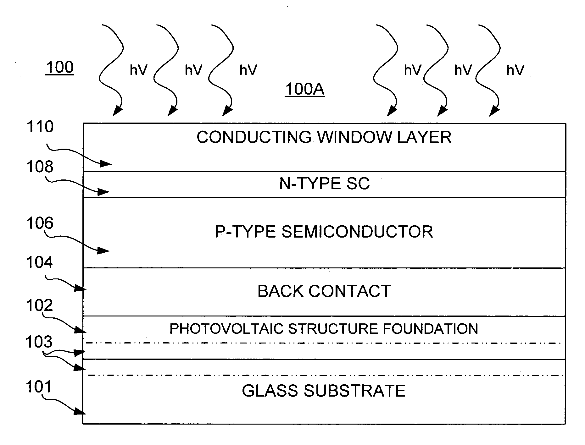
In contrast to microelectronic applications of SOI structures, photovoltaic structures are more tolerant of such defects, although such defects nonetheless adversely may affect performance of the photovoltaic cell.
While such finishing techniques as CMP and FA may improve surface characteristics, the defect-tolerance of photovoltaic structures may make them cost-prohibitive.

Method used


Image

  • Thin film photovoltaic structure
  • Thin film photovoltaic structure
  • Thin film photovoltaic structure

Examples


Embodiment Construction

[0091]Referring to FIGS. 4, 5 and 6, occasionally referred to collectively as FIGS. 4-6, there are shown PVS variations 100A, 100B and 100C, respectively, of photovoltaic SOI structure 100 in accordance with one or more embodiments of the present invention. Photovoltaic SOI structure 100 may be referred to as a PV SOI structure 100, or simply PVS 100. With respect to the figures, the SOI structure 100 is exemplified as an SiOG structure. The SiOG structure 100 may include an insulator substrate 101 made of glass, a photovoltaic structure foundation 102 (FIG. 4), ion migration zones 103, a back contact layer 104, a p-type semiconductor layer 106, an n-type semiconductor layer 108, and a conducting window layer 110. The SiOG structure 100 has suitable uses in connection with photovoltaic devices.

[0092]The conducting window layer 110 is an electrically conductive layer of material that is acting as an ohmic contact. The conducting window layer may be translucent, transparent or semi-tr...


PUM


Abstract

Systems and methods of production of a photovoltaic device include creating on a donor semiconductor wafer an exfoliation layer and transferring the exfoliation layer to an insulator substrate. One or more finishing processes may be performed before and / or after transferring the exfoliation layer, such as to create a plurality of photovoltaic structure layers. Production of the photovoltaic device further may include subjecting the donor semiconductor wafer to an ion implantation process to create the exfoliation layer, bonding the exfoliation layer to the insulator substrate, and separating the exfoliation layer from the donor semiconductor wafer. Transferring may include forming an anodic bond via electrolysis, such as through the application of heat, pressure and voltage to the exfoliation layer and the insulator structure.

Description

CROSS-REFERENCE TO RELATED APPLICATIONS[0001]The present invention claims the benefit of the filing date of the prior-filed U.S. Provisional Patent Application No. 60 / 810061 filed on May 31, 2006 by David Francis Dawson-Elli et al. and entitled “SINGLE CRYSTAL THIN FILM PHOTOVOLTAIC STRUCTURE,” the content of which is relied upon and incorporated herein by reference in its entirety.BACKGROUND[0002]1. Field Of Invention[0003]The present invention relates to the systems, methods and products of manufacture of a thin film photovoltaic structure, preferably having a substantially single crystal thin film, using improved processes, including in particular transferring photovoltaic structure foundations or partially completed photovoltaic structures to insulator substrates and anodic bonding to the insulator substrates.[0004]2. Description of Related Art[0005]Overview of Photovoltaics[0006]Photovoltaic structures (PVS) are a specialized form of semiconductor structure that converts photon...

Claims


Application Information

Patent Timeline
IPC IPC(8): H01L31/00
CPCH01L31/0687H01L31/078Y02E10/544H01L31/1896H01L31/18H01L21/2007
Inventor DAWSON-ELLI, DAVID FRANCISGADKAREE, KISHOR PURUSHOTTAMWALTON, ROBIN MERCHANT
Owner CORNING INC
Why Eureka
Try Eureka