
Resist composition and patterning process

a composition and resist technology, applied in the field of resist composition and patterning process, can solve the problems of ped [post exposure delay], defective accompanying of resist compositions, and thickening of upper portions, and achieve excellent etching resistance, improve perpendicularity of line patterns, and improve the effect of resolution

Active Publication Date: 2010-01-14
SHIN ETSU CHEM IND CO LTD
View PDF14 Cites 35 Cited by
  • Summary
  • Abstract
  • Description
  • Claims
  • Application Information

AI Technical Summary

Benefits of technology

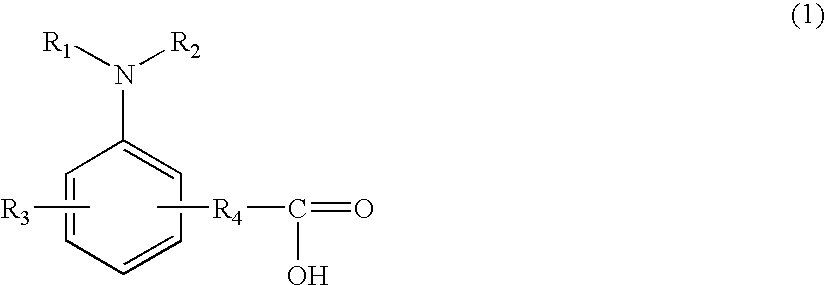
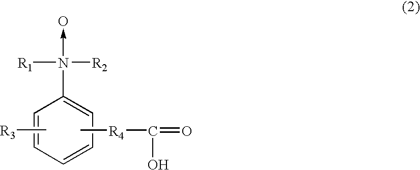
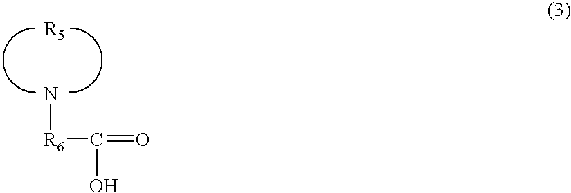
[0014]The present invention has been carried out in view of the above circumstances, and it is therefore an object of the present invention to provide: a resist composition for (1) a chemically amplified positive resist composition, which is made soluble in alkali upon elimination of an acid labile group by an acid catalyst, and (2) a chemically amplified negative resist composition, which is made insoluble in alkali by an acid catalyst and / or which is made insoluble in alkali by reaction with a crosslinking agent by an acid catalyst, such that the resist composition provides, by addition of the above-mentioned basic component, an excellent pattern profile even at a substrate-side boundary face of resist, in addition to a higher resolution in photolithography for micro-fabrication, and particularly in photolithography adopting, as an exposure source, KrF laser, ArF laser, F2 laser, ultra-short ultraviolet light, electron beam, X-rays, or the like; and a patterning process utilizing the resist composition.
[0015]To achieve the above object, the present inventors have earnestly conducted investigations to narrowly carry out the present invention, by resultingly finding that: adoption of an amine compound or amine oxide compound having a carboxyl group and having no hydrogen atoms covalently bonded to a nitrogen atom as a basic center as a basic component, to be added into a resist composition, allows for formation of a resist film, which resist film is capable of remarkably improving perpendicularity of a line pattern even at a substrate-side boundary face of resist in addition to a higher resolution, and which resist film provides an excellent etching resistance for preserving a pattern profile.

Problems solved by technology

However, chemically amplified resist compositions are defectively accompanied by: a problem (called PED [Post Exposure Delay]) such that extended standing-still periods from exposure to PEB (post-exposure bake) lead to T-topped shapes of line patterns upon formation of positive patterns, i.e., lead to patterns having thickened upper portions; or a problem, which is a so-called footing phenomenon where patterns are thickened near a substrate, such as a substrate formed with metal like Al, Cr, or the like, or a basic substrate, particularly a silicon nitride substrate or titanium nitride substrate.
Although it has been proposed to use a relatively weak base against the above-mentioned T-topped problem, the weak base is insufficient for control of deprotection reaction within a resist film, i.e., for control of diffusion of acids for causing a catalytic reaction, in case of adoption of acid labile groups having higher reactivities to be used for obtaining higher resolutions.
Addition of weak base particularly results in progression of dark reaction in PED even at an non-exposed area, thereby causing a decrease of line dimension (slimming) and a film decrease at line surface in PED.
However, stronger basicities are not necessarily preferable, such that a sufficient effect can not be obtained even by addition of DBU (1,8-diazabicyclo[5.4.0]-7-undecene) or DBN (1,5-diazabicyclo[4.3.0]-5-nonene), which are regarded as being super base, or proton sponge (1,8-bis(dimethylamino)naphthalene), or quaternary ammonium hydroxides such as tetramethylammonium hydroxide.
Concerning pattern profile in substrate-side boundary face of resists, although problems of footing profile and undercut are improved by addition of base, the improvement is insufficient.
While further increase of addition amounts of base will result in further improvement, there is caused a tradeoff problem of a considerably deteriorated sensitivity.
However, the countermeasure on a substrate side requires an increased number of steps for processing, and is problematic not only in a complicated process but also in an increased production cost.
However, adoption of the low vapor pressure base leads to evaporation of the base at a prebaking temperature, thereby occasionally causing a sensitivity change by a concentration change.
This makes it difficult to keep dimensions of a pattern with higher precision.
However, there have not been found important proposals thereafter to use such an amine compound having a carboxyl group, and such a situation is considered to be due to failure of remarkable effects by such usage in seeking for a higher resolution.

Method used


Image

  • Resist composition and patterning process
  • Resist composition and patterning process
  • Resist composition and patterning process

Examples


examples

[0354]The present invention will be concretely explained by describing Examples and Comparative Examples, concerning the resist composition including the amine compound or amine oxide compound having a carboxyl group and having no hydrogen atoms covalently bonded to a nitrogen atom as a basic center, without limited to the Examples.

[0355]Shown below are structural formulae of base resins (Polymers 1 and 2) and acid generators (PAG-1,2) as constituent materials of resist compositions, used in the present invention. In the following Examples, Mw and Mn represent values determined relative to polystyrene standards, as measured by gel permeation chromatography (GPC).

[0356]Solvent (A): propylene glycol methyl ether acetate (PGMEA)

[0357]Solvent (B): ethyl lactate (EL)

[0358]Further, the following compounds are amine compounds or amine oxide compounds having a carboxyl group and having no hydrogen atoms covalently bonded to a nitrogen atom as a basic center, and other inapplicable basic com...

examples 1 to 6

, and Comparative Examples 1 to 3

[0381]Resist compositions listed in Table 1 were dissolved in the listed solvents, respectively, and the obtained resist compositions were each filtered by a filter of 0.04 μm size made of nylon resin, followed by spin coating of each resist solution at a revolution speed of 2,500 rpm onto a mask blank of 152 mm square having an outermost surface made of chromium oxide nitride, into a coated thickness of 150 nm. Next, each mask blank was baked for 10 minutes by a hot plate at 90° C. Measurement of a thickness of each obtained resist film was conducted by an optical measurement device NanoSpec (manufactured by Nanometrics Incorporated). The measurement was conducted at 81 in-plane points of an applicable blank substrate except for an outer peripheral region from an outer edge to an inner extent at a distance of 10 mm therefrom, so as to calculate an averaged film thickness and a film thickness range.

TABLE 1Composition(weightCom.Com.Com.part)Ex. 1Ex. 2...

example 7 to example 15

[0386]Resist compositions listed in Table 3 were prepared, which included the amine compound having a carboxyl group and having no hydrogen atoms covalently bonded to a nitrogen atom as a basic center of the present invention, and the conventional amine compounds, and the patterning process of the present invention was performed for them in the same manner as Examples 1 through 6 to conduct evaluation of resolutions and pattern profiles thereof. Results thereof are listed in Table 4. In all Examples, excellent resolutions, pattern profiles without footing, and excellent line edge roughness were obtained.

TABLE 3Composition(weightEx.Ex.Ex.Ex.Ex.Ex.part)Ex. 7Ex. 8Ex. 9101112131415polymer-1808080808080808080PAG-1666666666PAG-2222222222Quencher-20.10.10.10.10.10.10.10.10.1Quencher-0.1————0.05———10Quencher-—0.1————0.050.050.0511Quencher-——0.1——0.0512Quencher-———0.1—0.05—0.05—13Quencher-————0.10.05——14Surfactant A0.070.070.070.070.070.070.070.070.07Solvent A470470470470470470470470470Solve...


PUM

PropertyMeasurementUnit
Fractionaaaaaaaaaa
Fractionaaaaaaaaaa
Fractionaaaaaaaaaa

Abstract

The present invention relates to: a resist composition such as a chemically amplified resist composition for providing an excellent pattern profile even at a substrate-side boundary face of resist, in addition to a higher resolution in photolithography for micro-fabrication, and particularly in photolithography adopting, as an exposure source, KrF laser, ArF laser, F2 laser, ultra-short ultraviolet light, electron beam, X-rays, or the like; and a patterning process utilizing the resist composition. The present invention provides a chemically amplified resist composition comprising one or more kinds of amine compounds or amine oxide compounds (except for those having a nitrogen atom of amine or amine oxide included in a ring structure of an aromatic ring) at least having a carboxyl group and having no hydrogen atoms covalently bonded to a nitrogen atom as a basic center.

Description

BACKGROUND OF THE INVENTION[0001]1. Field of the Invention[0002]The present invention relates to a photoresist to be used for micro-fabrication of semiconductors, photomask blanks, and the like, and particularly to a chemically amplified positive or negative resist to be used for precisely conducting micro-fabrication by ultraviolet rays, EUV, electron beam exposure at wavelengths of 300 nm or shorter. Description of the Related Art:[0003]It is known that finer pattern rules are demanded with highly integrated LSI's providing highly increased speeds. This has correspondingly led to largely changed exposure methods and resist compositions, and particularly, KrF, ArF excimer laser light, electron beam, and the like are used as exposure light sources upon conduction of lithography of patterns at 0.2 μm or less, in a manner to adopt chemically amplified photoresists, which exhibit excellent sensitivities to such high energy radiations and provide higher resolutions.[0004]However, chemic...

Claims


Application Information

Patent Timeline
IPC IPC(8): G03F7/00C07C229/00
CPCG03F7/0045Y10S430/114Y10S430/128G03F7/0382G03F7/004G03F7/0047G03F7/039G03F7/0397G03F7/0392
Inventor WATANABE, SATOSHITANAKA, AKINOBUWATANABE, TAKERUKINSHO, TAKESHI
Owner SHIN ETSU CHEM IND CO LTD
Learn More