
Photosensitive resist underlayer film forming composition

a technology of resist and film, applied in the field of resist underlayer film, can solve the problems of lowering the dimensional accuracy of the photoresist pattern, difficult to keep the film thickness of the photoresist large enough for the processing of the substrate, and performing dry etching, etc., and achieve the effect of shortening the diffusion length of the strong acid

Active Publication Date: 2011-12-22
NISSAN CHEM IND LTD
View PDF7 Cites 10 Cited by
  • Summary
  • Abstract
  • Description
  • Claims
  • Application Information

AI Technical Summary

Benefits of technology

Part of the acid generated by the photoacid generator in the resist film during the exposure is considered to move also into the resist underlayer film. Meanwhile, a photoacid generator also exists in the resist underlayer film, and at the interface, a large amount of acids is easily formed. Such excessive acid moves to an unexposed portion and the unexposed portion exhibits alkali solubility, and the pattern is deformed as a result. To prevent such pattern deformation, a basic compound assuming a role of trapping excessive acid such as amines can be mixed in the composition. By mixing a long-chain fluoroalkylcarboxylic acid or a salt of the fluoroalkylcarboxylic acid as the (D) component in the composition in the present invention, the resist underlayer film has a buffer and ph of the resist underlayer film does not largely vary in spite of excessive acid, Therefore, the =exposed portion does not exhibit alkali solubility and thus it is considered that the resist shape becomes a rectangular shape. In addition, a weak carboxylic acid derived from a long-chain fluoroalkylcarboxylic acid or a salt of the fluoroalkylcarboxylic acid existing in the resist underlayer film interacts strongly with a strong acid generated by a photoacid generator and shortens a diffusion length of the strong acid. Consequently, the transition of the excessive acid into the unexposed portion is suppressed and the resist shape is considered to be a rectangular shape.

Problems solved by technology

However, these photolithography processes can cause a problem of lowering the dimensional accuracy of a photoresist pattern due to the influence of a standing wave caused by the reflection of exposure light on the substrate or the influence of the diffuse reflection of exposure light caused by unevenness of the substrate.
However, the photoresist is also dry etched in the removal process of the bottom anti-reflective coating by dry etching, which makes it difficult to keep the film thickness of the photoresist large enough for the processing of the substrate.
This becomes a critical problem especially when a thin film photoresist is used to enhance the resolution.
In this process, to prevent the surface of a substrate from being damaged, it is not desired to perform dry etching in the formation of a photoresist pattern.
Therefore, in the formation of a photoresist pattern for an ion implantation process, a bottom anti-reflective coating requiring the removal by dry etching cannot be used as an underlayer of the photoresist.
Therefore, in terms of the applicability to fine processing and the shape of a pattern to be formed, such bottom anti-reflective coating is not satisfactory.

Method used


Image

  • Photosensitive resist underlayer film forming composition
  • Photosensitive resist underlayer film forming composition
  • Photosensitive resist underlayer film forming composition

Examples


example

Synthesis Example 1

20 g of N-(4-hydroxyphenyl)methacrylamide (manufactured by Tokyo Chemical Industry Co., Ltd.), 11.148 g of 4-vinylbenzoic acid (manufactured by Tokyo Chemical Industry Co., Ltd.), 17.327 g of 9-anthracenemethyl methacrylate (manufactured by Osaka Organic Chemical Industry Ltd.), and 4.8 g of 2,2′-azobis(isobutyric acid)dimethyl (manufactured by Wako Pure Chemical Industries, Ltd.) were dissolved in 124.4 g of methanol. The resultant reaction solution was dropped into 90 g of methanol warmed to 70° C. over 10 hours. Then, while maintaining the resultant reaction mixture at 70° C., the reaction was effected for 12 hours. The resultant reaction mixture was charged into ethyl acetate to precipitate a polymer. The obtained powder polymer was dried under reduced pressure to produce 42.5 g of a polymer of Formula (8-1):

The obtained polymer was subjected to a GPC analysis and as the result of the analysis, the polymer was found to have a weight average molecular weight of...

synthesis example 2

20 g of 4-acetoxystyrene (manufactured by Tosoh Corporation), 4.55 g of methacrylic acid, and 2.46 g of 2,2′-azobis(isobutyric acid)dimethyl (manufactured by Wako Pure Chemical Industries, Ltd.) were dissolved in 63 g of tetrahydrofuran. The resultant reaction solution was dropped into 45 g of tetrahydrofuran warmed to 70° C. over, 10 hours. Then, while maintaining the resultant reaction mixture at 70° C., the reaction was effected for 12 hours. The resultant reaction mixture was charged into hexane to precipitate a polymer. Next, 10 g of the obtained polymer and 3 g of triethylamine were dissolved in 3 g of water, 30 g of methanol, and 30 g of tetrahydrofuran, and the resultant reaction solution was heated to reflux for 14 hours, followed by returning the reaction solution to room temperature to concentrate the reaction solution. Then, the resultant reaction mixture was re-dissolved in 30 g of acetone, to which 3 g of acetic acid was added. Next, the resultant reaction solution was...

example 1

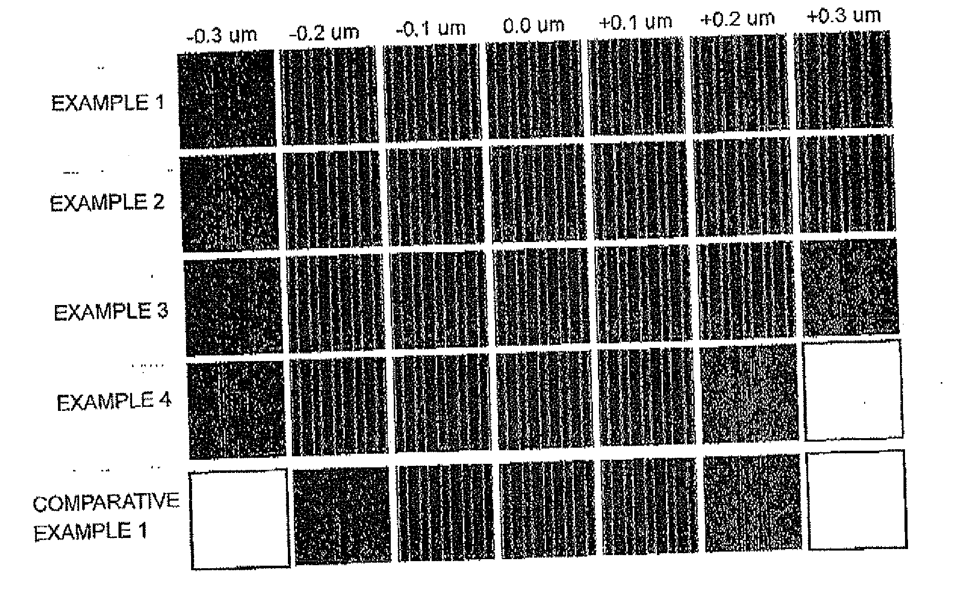
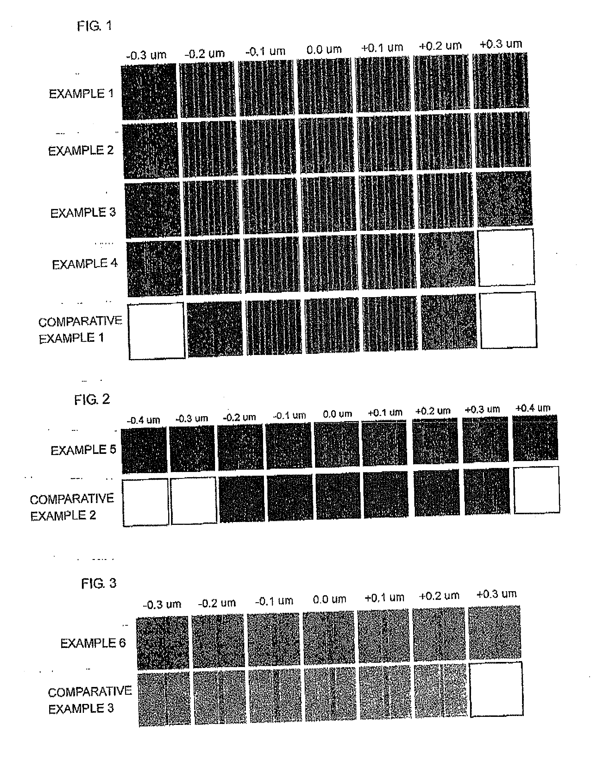
0.1 g of the polymer obtained in Synthesis Example 1 as (A) was mixed with 0.04 g of 1,3,5-tris(4-vinyloxybutyl)trimellitate (Formula (4-2)) as (B), 0.0058 g of triphenylsulfonium triflate (manufactured by Midori Kagaku. Co., Ltd.; trade name: TPS-105; Formula (8-3) below) as (C), 0.0038 g of N-lauryldiethartolamine (manufactured by Tokyo Chemical Industry Co., Ltd.) as (F), and 0.0098 g of triphenylsulfonium pentadecafluorooctanoate (manufactured by Wako Pure Chemical Industries, Ltd.; trade name: WPAG-422; Formula (8-4) below) as (1)), and the resultant mixture was dissolved in 8.9 g of propylene glycol monomethyl ether as (E). Subsequently, the resultant solution was filtered using a polyethylene microfilter having a pore diameter of 0.10 μm, and further filtered using a polyethylene microfilter having a pore diameter of 0.05 μm to prepare a photosensitive resist underlayer film forming composition (solution).


PUM

PropertyMeasurementUnit
wavelengthaaaaaaaaaa

Abstract

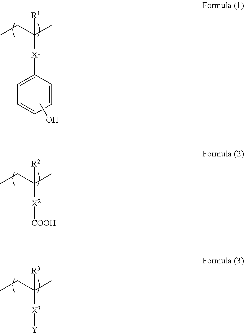
A resist underlayer film forming composition used in a lithography process includes: a polymer (A) containing a unit structure having a hydroxy group, a unit structure having a carboxy group, or combination thereof; a crosslinkable compound (B) having at least two vinyl ether groups; a photoacid generator (C); a C4-20 fluoroalkylcarboxylic acid or a salt of the fluoroalkylcarboxylic acid (D); and a solvent (E). The polymer (A) includes a unit structure selected from unit structures of Formula (1), Formula (2), and Formula (3);

Description

BACKGROUND OF THE INVENTION1. Field of the InventionThe present invention relates to a resist underlayer film used in a lithography process during the production of a semiconductor device and to a forming method of a resist pattern using the resist underlayer film.2. Description of the Related ArtIn the production of a semiconductor device, fine processing by lithography using a photoresist is performed. The fine processing is a processing method for forming fine convexoconcave corresponding to a pattern on the surface of a substrate by: forming a thin film of a photoresist on a semiconductor substrate such as a silicon wafer; irradiating the resultant thin film with an activating light ray such as an ultra violet ray through a mask pattern in which a pattern of a device is depicted; developing the film; and subjecting the substrate to etching processing using the resultant photoresist pattern as a protection film. Recently, higher integration of devices has been pursued, and there ...

Claims


Application Information

Patent Timeline
Patent Type & Authority Applications(United States)
IPC IPC(8): G03F7/004G03F7/20
CPCG03F7/0045G03F7/0046G03F7/095G03F7/091G03F7/0392
Inventor KIMURA, SHIGEONISHIMAKI, HIROKAZUOHASHI, TOMOYAUSUI, YUKIKISHIOKA, TAKAHIRO
Owner NISSAN CHEM IND LTD
Learn More