Three-dimensional multi-gate high-voltage N type transverse double-diffused metal-oxide semiconductor device
A lateral double diffusion, semiconductor tube technology, used in semiconductor devices, semiconductor/solid-state device manufacturing, electrical components, etc., can solve the problems of not maximizing the use of chip area, small on-resistance, large saturation current, etc., to achieve improved performance , The effect of good breakdown characteristics and good temperature characteristics
- Summary
- Abstract
- Description
- Claims
- Application Information
AI Technical Summary
Problems solved by technology
Method used
Image
Examples
Embodiment 1
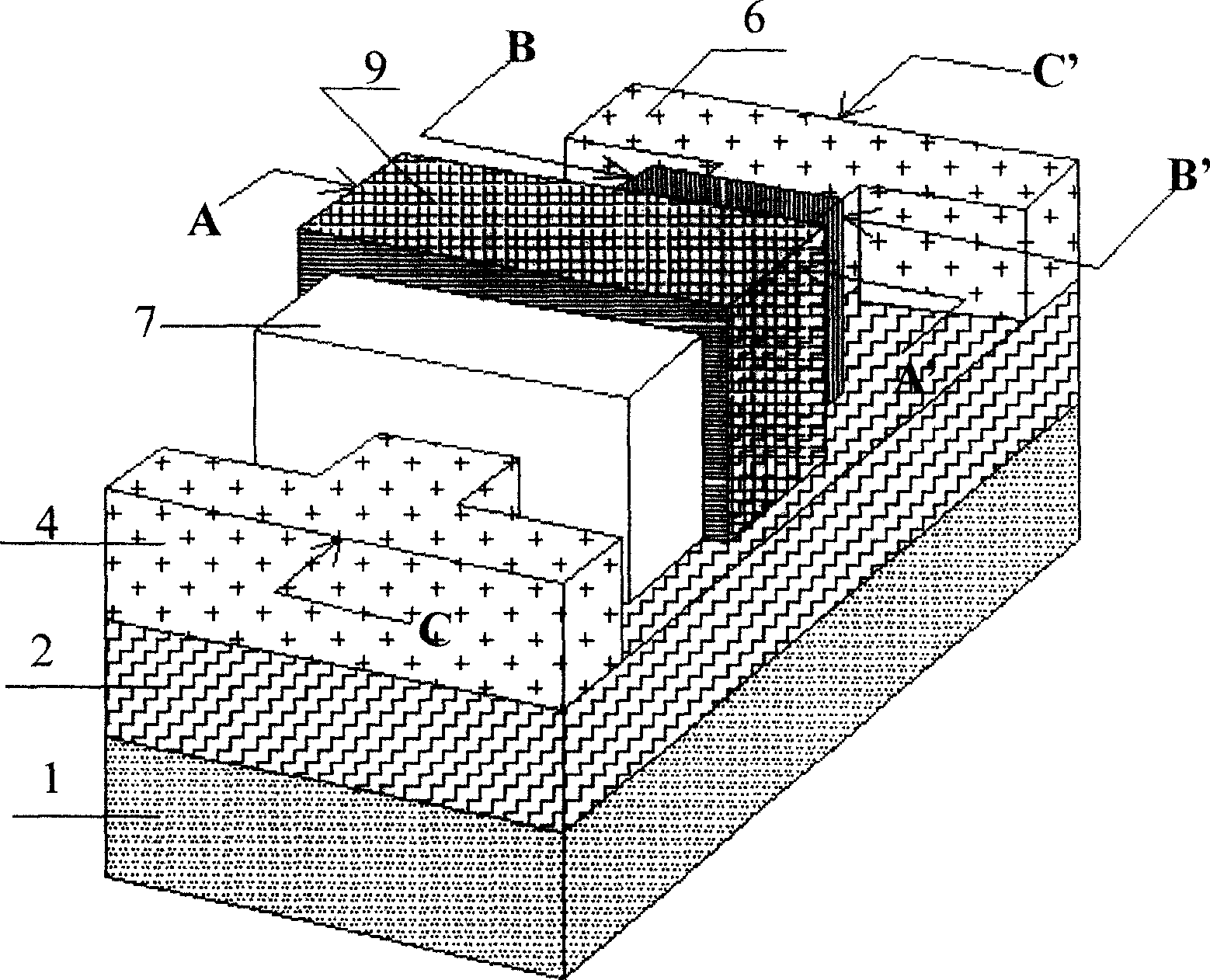
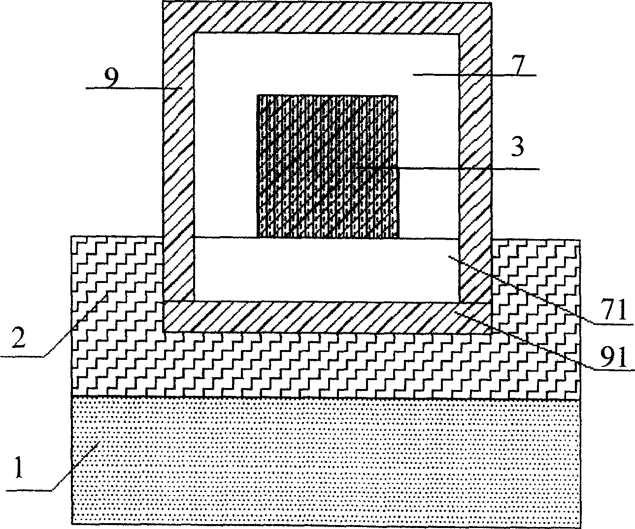
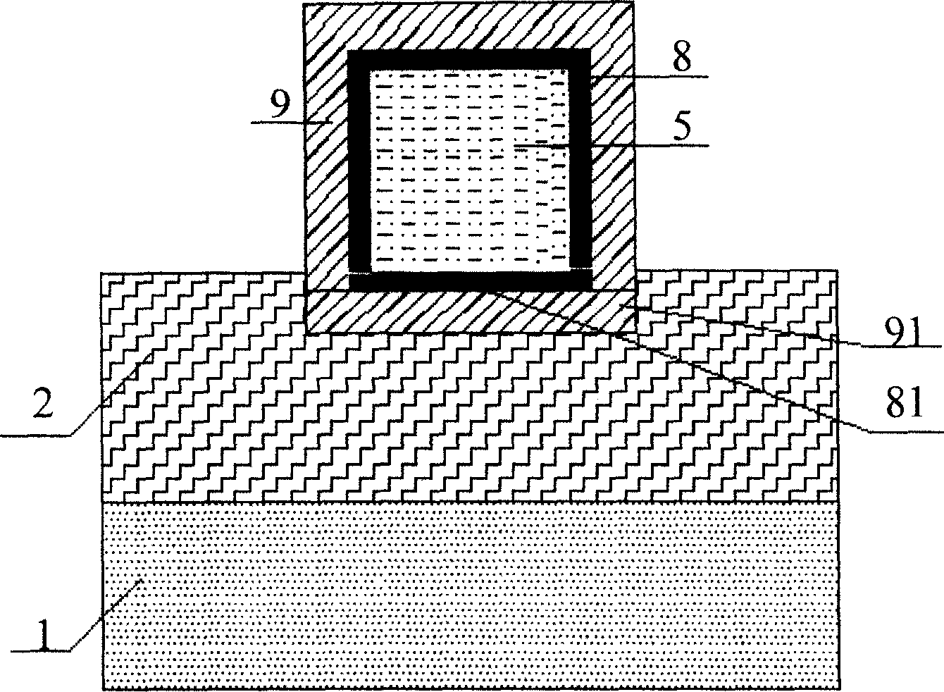
[0019] A three-dimensional multi-gate high-voltage N-type lateral double-diffused metal oxide semiconductor transistor used as a high-voltage device, comprising: a P-type substrate 1, an oxide layer 2 is arranged on the P-type substrate 1, and an oxide layer is arranged on the oxide layer 2. A columnar N-type drift region 3, on the oxide layer 2 and located adjacent to both ends of the N-type drift region 3, an N-type drain 4 and an N channel 5 are respectively arranged, on the oxide layer 2 and located adjacent to the N channel 5 An N-type source 6 is provided at the position, a field oxide layer 7 is coated on the surface of the N-type drift region 3, a gate oxide layer 8 is coated on the surface of the N channel 5, and the surfaces of the field oxide layer 7 and the gate oxide layer 8 are Coated with a polysilicon layer 9, in this embodiment, a cavity 21 is provided on the oxide layer 2 and below the N-type drift region 3 and the N channel 5, and a field oxide bottom layer 7...
Embodiment 2
[0021] A preparation process for manufacturing the three-dimensional multi-gate high-voltage N-type lateral double-diffused metal oxide semiconductor tube described in claim 1, characterized in that a P-type substrate is prepared first, and then an oxide layer is prepared on the P-type substrate. P-type silicon is grown on the oxide layer, N-type doping is performed on a part of the P-type silicon to form an N-type drift region, and a field oxide layer is formed on the two sides and the upper surface of the N-type drift region by wet thermal oxidation. P-type doping is carried out on the P-type silicon to form an N-type channel, and dry thermal oxidation is grown on both sides and the upper surface of the N-type channel to form a gate oxide layer. Deposit polysilicon and form a polysilicon layer on the surface and part of the both side surfaces and the upper surface of the N-type drift region. Finally, perform source and drain N-type impurity implantation, engrave holes and pre...
PUM
| Property | Measurement | Unit |
|---|---|---|
| Thickness | aaaaa | aaaaa |
| Thickness | aaaaa | aaaaa |
Abstract
Description
Claims
Application Information
 - R&D
- Intellectual Property
- Life Sciences
- Materials
- Tech Scout
- Unparalleled Data Quality
- Higher Quality Content
- 60% Fewer Hallucinations
Browse by: Latest US Patents, China's latest patents, Technical Efficacy Thesaurus, Application Domain, Technology Topic, Popular Technical Reports.
© 2025 PatSnap. All rights reserved.Legal|Privacy policy|Modern Slavery Act Transparency Statement|Sitemap|About US| Contact US: help@patsnap.com


