
High-power infrared semiconductor diode light emitting device

a light-emitting device and infrared technology, applied in semiconductor lasers, lasers, active medium materials, etc., can solve the problems of high modulation speed and output power exceeding that of telecommunication lasers, and achieve high modulation speed, minimize the effect of elevated active layer temperature on laser efficiency, and minimize the effect of temperature rise of the active region

Active Publication Date: 2010-04-20
SEMINEX CORP
View PDF15 Cites 4 Cited by
  • Summary
  • Abstract
  • Description
  • Claims
  • Application Information

AI Technical Summary

Benefits of technology

[0008]The invention is a semiconductor laser diode using aluminum gallium indium arsenide, gallium indium arsenide phosphide, indium phosphide, (AlGaInAs / GaInAsP / InP) material system and related combinations. Both the design of the active layer and the design of the optical cavity are optimized to minimize the temperature rise of the active region and to minimize the effects of elevated active layer temperature on the laser efficiency. The result is a high output power semiconductor laser for the wavelengths between 1.30 and 1.61 micrometers. The output power exceeds that exhibited by telecommunication lasers, which are required to have high modulation speeds at the expense of output power.
[0009]In one embodiment, the active layer of the inventive device is a strain compensated multiquantum well structure comprising an intraplanar compressively strained AlGaInAs well and a tensile strained AlGaInAs barrier layer. The thickness of the quantum well is 7 nanometers (nm) or less. The strain is chosen to maximize the conduction band discontinuity while still staying below the critical thickness limit to preclude dislocation formation, so that at high operating temperatures electrons are not lost to the confinement layer due to thermal emission. The width of the well is adjusted to achieve the desired operating wavelength within the constraints of the critical layer thickness.
[0012]Another aspect of the invention is the selection of the number of quantum wells in the active layer so as to minimize the thermal power dissipation density in the active layer, combined with a longer cavity length and cavity width to achieve sufficient gain so that a high optical output power is obtained. Because the area of the junction is larger, the thermal resistance is reduced, thereby resulting in a lower junction temperature for the laser operation at a given output power.

Problems solved by technology

The output power exceeds that exhibited by telecommunication lasers, which are required to have high modulation speeds at the expense of output power.

Method used


Image

  • High-power infrared semiconductor diode light emitting device
  • High-power infrared semiconductor diode light emitting device
  • High-power infrared semiconductor diode light emitting device

Examples


Embodiment Construction

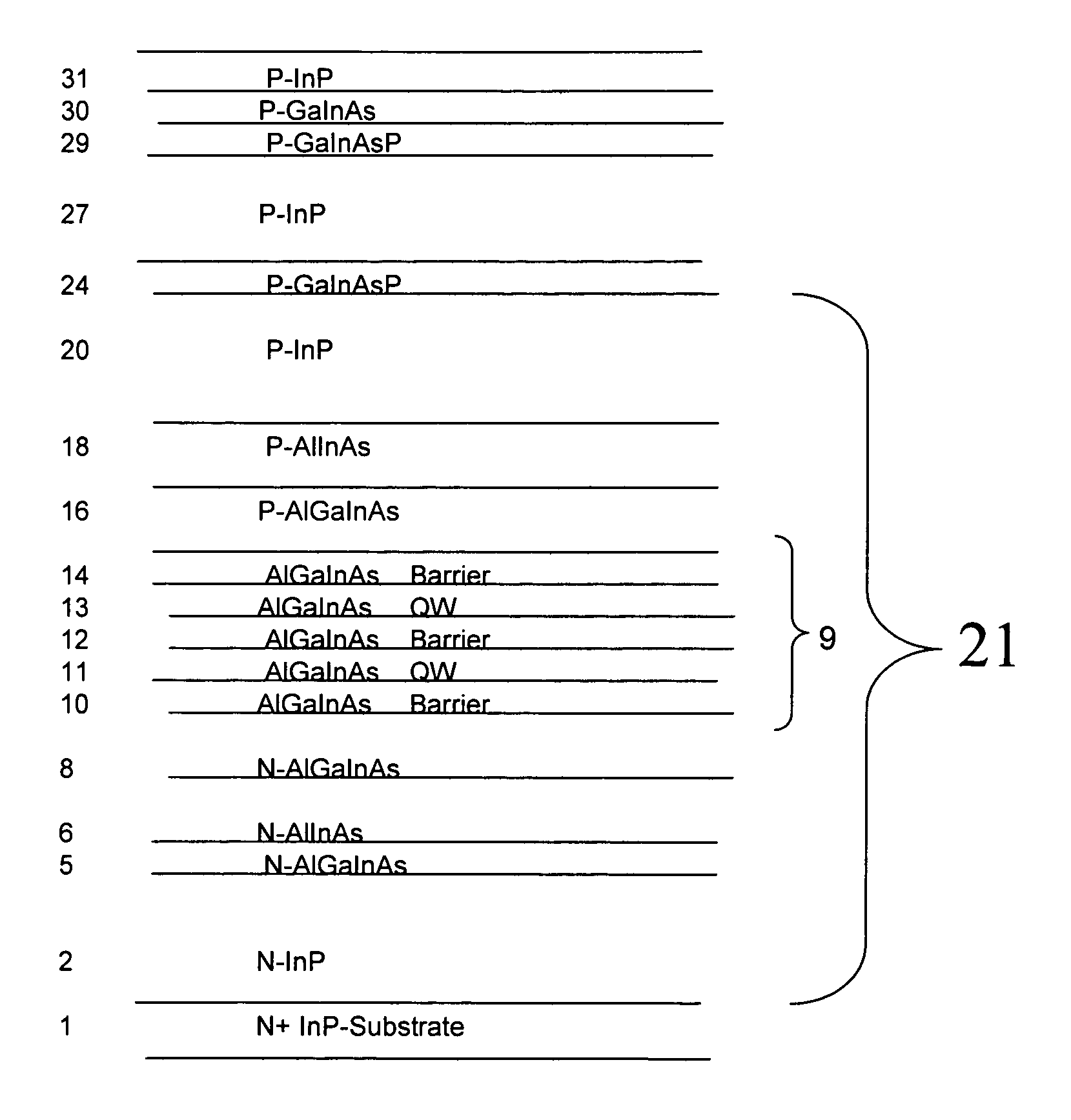
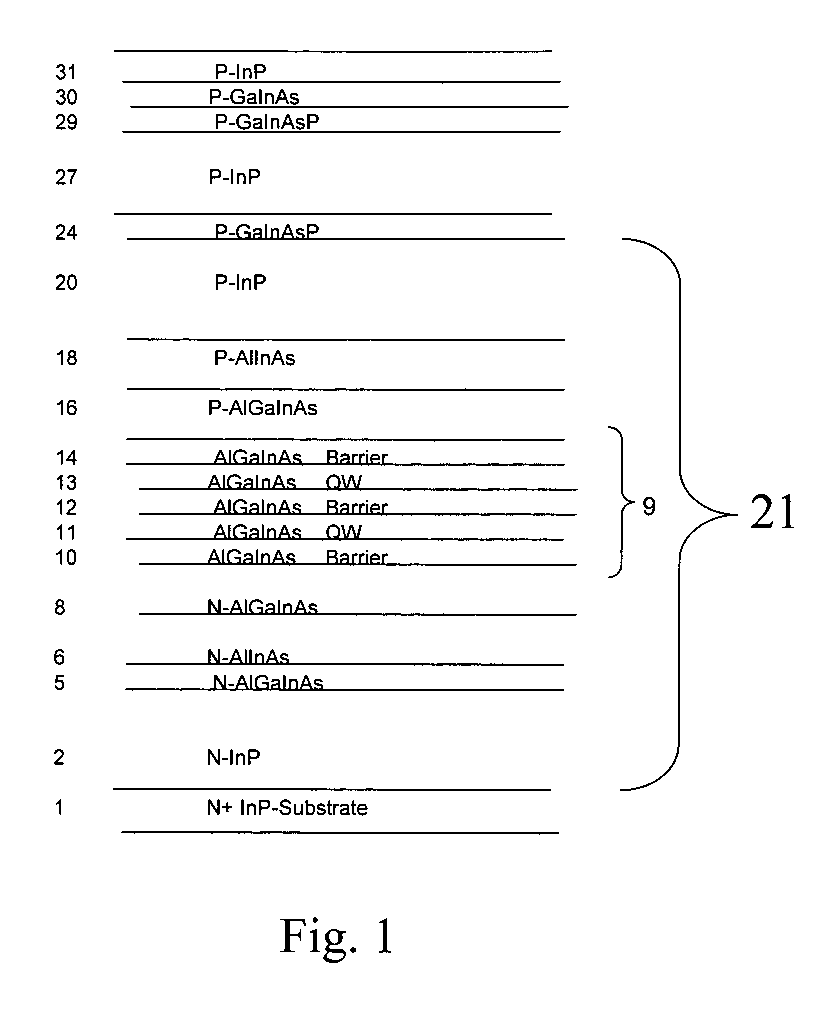
[0023]FIG. 1 shows the layer structure of a semiconductor light emitting device that has been constructed according to the principles of the present invention.

[0024]Specifically, a listing of the epitaxial structure shown. It was fabricated or prepared using conventional III-V compound semiconductor epitaxial growth techniques such as metal organic chemical vapor deposition OMCVD (also referred to as MOCVD) and molecular beam epitaxy (MBE). The starting substrate 1 is n-type InP, on to which the sequence of layers is epitaxially grown using known methods.

[0025]Beginning from the substrate 1, a 1 micrometer thick n+InP lower cladding layer 2 with a silicon (Si) doping concentration of 3×1018 cm−3 is grown followed by a transition region 15 nm thick of lattice matched, graded (Al0.68Ga0.32)0.47In0.53As to Al0.48In0.52As 5-6 into the separate confinement heterostructure (SCH) layers 6-18. Next is the lower graded-index (GRIN) layer 8, which is 45 nm thick beginning with Al0.48In0.52As ...


PUM


Abstract

A semiconductor laser diode using the aluminum gallium, arsenide, gallium indium arsenide phosphide, indium phosphide, (AlGaInAs / GaInAsP / InP) material system and related combinations is disclosed. Both the design of the active layer and the design of the optical cavity are optimized to minimize the temperature rise of the active region and to minimize the effects of elevated active layer temperature on the laser efficiency. The result is a high output power semiconductor laser for the wavelengths between 1.30 and 1.61 micrometers for the pumping of erbium doped waveguide devices or for direct use in military, medical, or commercial applications.

Description

RELATED APPLICATIONS[0001]This application claims the benefit of U.S. Provisional Application No. 60 / 612,112, filed on Sep. 23, 2004, which is incorporated herein by reference in its entirety.BACKGROUND OF THE INVENTION[0002]High gain, high-energy solid-state lasers that operate in the eye safe region (wavelength>1.3 micrometers) are in demand for military and commercial applications. These lasers, are typically based on crystals doped with erbium (Er) atoms that are pumped with semiconductor lasers at approximately 980 nanometers to achieve very high powers (power>3 watts). Semiconductor lasers using indium phosphide base material can also achieve laser light in this spectrum range, but at significantly lower powers (less than 1.5 Watts). There are several military requirements for such lasers. One is the augmentation of fire control systems with the capability to identify the target (Target ID) using laser radar (LADAR) imaging techniques. Another is the development of ultra...

Claims


Application Information

Patent Timeline
Patent Type & Authority Patents(United States)
IPC IPC(8): H01S3/04H01L31/00H01S3/14
CPCB82Y20/00H01S5/02461H01S5/22H01S5/2231H01S5/34313H01S5/34366H01S5/0224H01S5/02272H01S5/2004H01S5/2214H01S5/305H01S5/3054H01S5/3077H01S5/3215H01S5/3406H01S5/34306H01S5/0217H01S5/0234H01S5/0237
Inventor BEAN, DAVID M.QIAN, YIPULVER, DANIEL E.
Owner SEMINEX CORP
Learn More