Method and apparatus for a self-aligned heterojunction bipolar transistor using dielectric assisted metal liftoff process

a technology of heterojunction bipolar transistor and liftoff process, which is applied in the field of self-aligned heterojunction bipolar transistor, can solve the problems of insufficient reliability of hbt devices to incorporate these ics, the inability to completely symmetrical the transistor, etc., to achieve the effect of improving etch control, reducing the etching and sputtering of the emitter metal, and improving chemical vapor deposition

Inactive Publication Date: 2005-05-17
RJM SEMICON
View PDF4 Cites 9 Cited by
  • Summary
  • Abstract
  • Description
  • Claims
  • Application Information

AI Technical Summary

Benefits of technology

[0039]The disclosed invention provides a precise means of manufacturing compound semiconductor HBTs with self-aligned emitter and base metal contacts having submicron spacing using a dielectric-assisted metal liftoff process. Specifically, the method according to the invention uses an “H-shaped” dielectric film of, for example, Si3N4, SiO2, or SiOxNy that conformally covers the emitter metal contact post. This insulating layer is used as an etch mask to form the emitter electrical p-n junction. The insulator is then etched using HF etchant to remove excess base metal deposited on top of the emitter metal, which does not etch the emitter and base metal contact

Problems solved by technology

However, in practice, the transistor is not completely symmetrical.
In addition, HBTs may be used in phased-array radar and very high frequency terrestrial and satellite communication systems, and the reliability of HBT devices is not sufficient to incorporate these ICs into such applications, primarily due to the limitations of present HBT process technologies.
However, Si BJTs and SiGe HBTs suffer from several performance disadvantages in comparison to compound semiconductor HBTs, including, for example, low collector breakdown voltages and the inability to integrate passive components in ICs including resistors, capacitors, and inductors due to the glossy, conductive Si substrate.
Although the “T-shaped” emitter HBT has resulted in ICs with world record speeds in the research laboratory, they suffer from several different manufacturing and processing problems that will ultimately limit their use in commercial high-speed IC applications.
Also, the emitter undercut impedes the ability to deposit a conformal dielectric coating of Si3N4 and/or SiO2 that is considered to be essential for proper passivation of the emitter p-n junction.
The inability to completely fill the emitter undercut can result in significantly reduced reliability and lifetimes of the HBT device, thereby precluding their use in many IC applications.
Another significant disadvantage to the “T-shaped” emitter HBT process is that it also greatly impedes process control since the undercut of the emitter metal is hidden from the surface.
This makes it virtually impossible to accurately measure the undercut 8 in an HBT semiconductor process line.
However, AFM cannot be used to measure the emitter undercut in the “T-shaped” HBT process because the AFM probe tip cannot penetrate below the emitter metal in the emitter undercut region.
Also, SEM imaging of a tilted wafer cannot be used to accurately measure the emitter undercut due to the shadowing effect of the emitter metal in the collection of secondary electrons.
Another difficult and potentially fatal HBT reliability problem results from the use of conventional hydrochloric acid (HCl)-based wet etch chemistries to selectively etch the emitter layers containing AlInAs, InP, or InGaP regions while stopping at InGaAs or GaAs layers that form the p-type base layer.
Selective etches are often used in the emitter etch process to prevent over-etching into the base region that would lead to variations in the base resistance and thus greatly reduce IC yields.
The kinetics for etching with HCl-based wet chemical etches is reaction rate limited leading to highly anisotropic etch profiles.
The lack of complete dielectric pass

Method used


Image

  • Method and apparatus for a self-aligned heterojunction bipolar transistor using dielectric assisted metal liftoff process
  • Method and apparatus for a self-aligned heterojunction bipolar transistor using dielectric assisted metal liftoff process
  • Method and apparatus for a self-aligned heterojunction bipolar transistor using dielectric assisted metal liftoff process

Examples


Embodiment Construction

[0063]As required, a detailed illustrative embodiment of the present invention is disclosed herein. However, techniques, systems and operating structures in accordance with the present invention may be embodied in a wide variety of forms and modes, some of which may be quite different from those in the disclosed embodiment. Consequently, the specific structural and functional details disclosed herein are merely representative, yet in that regard, they are deemed to afford the best embodiment for purposes of disclosure and to provide a basis for the claims herein which define the scope of the present invention. It should be noted that those individuals skilled in the art may be able to make some modifications of the preferred embodiments but which are based upon the underlying teachings contained within this subject invention.

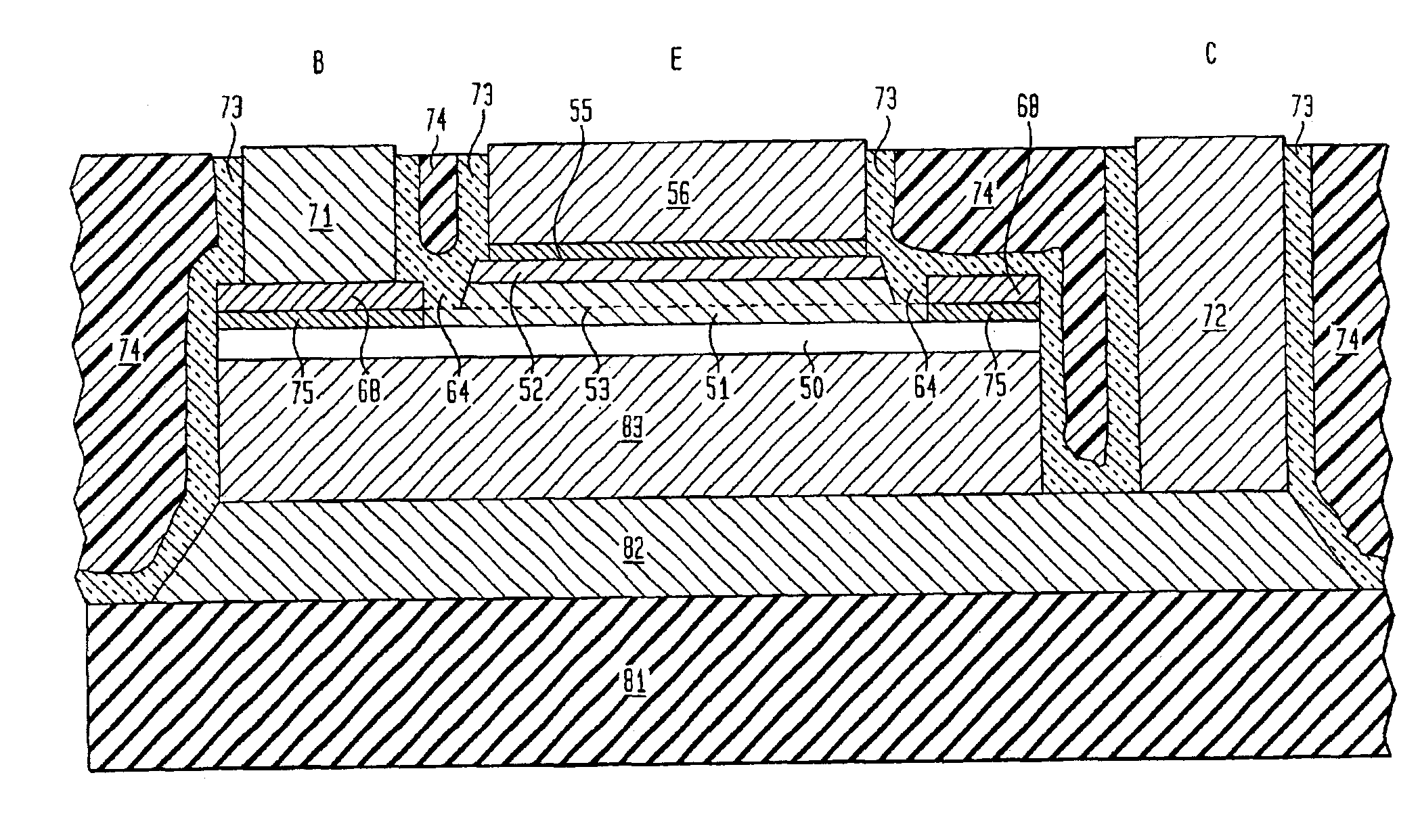
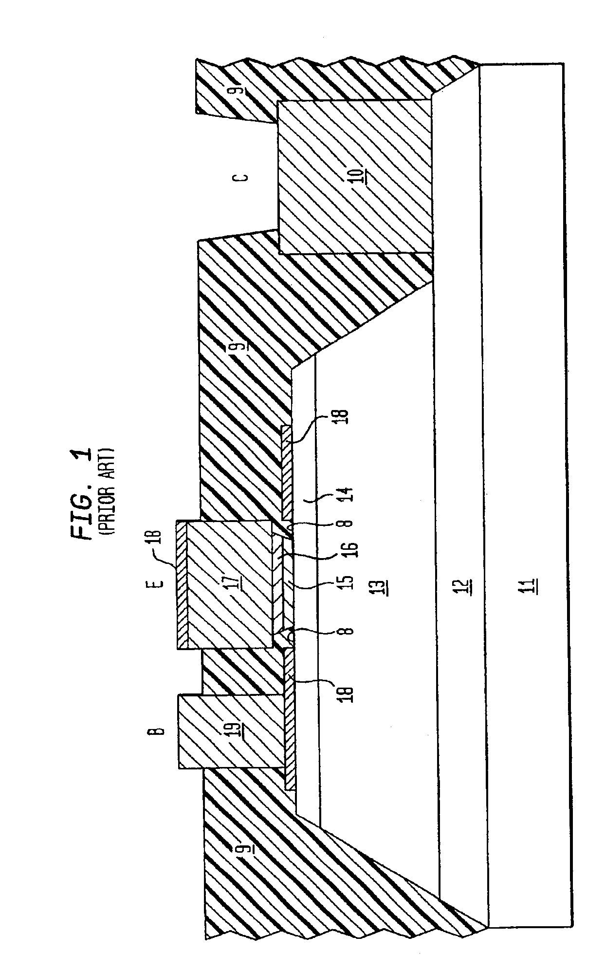
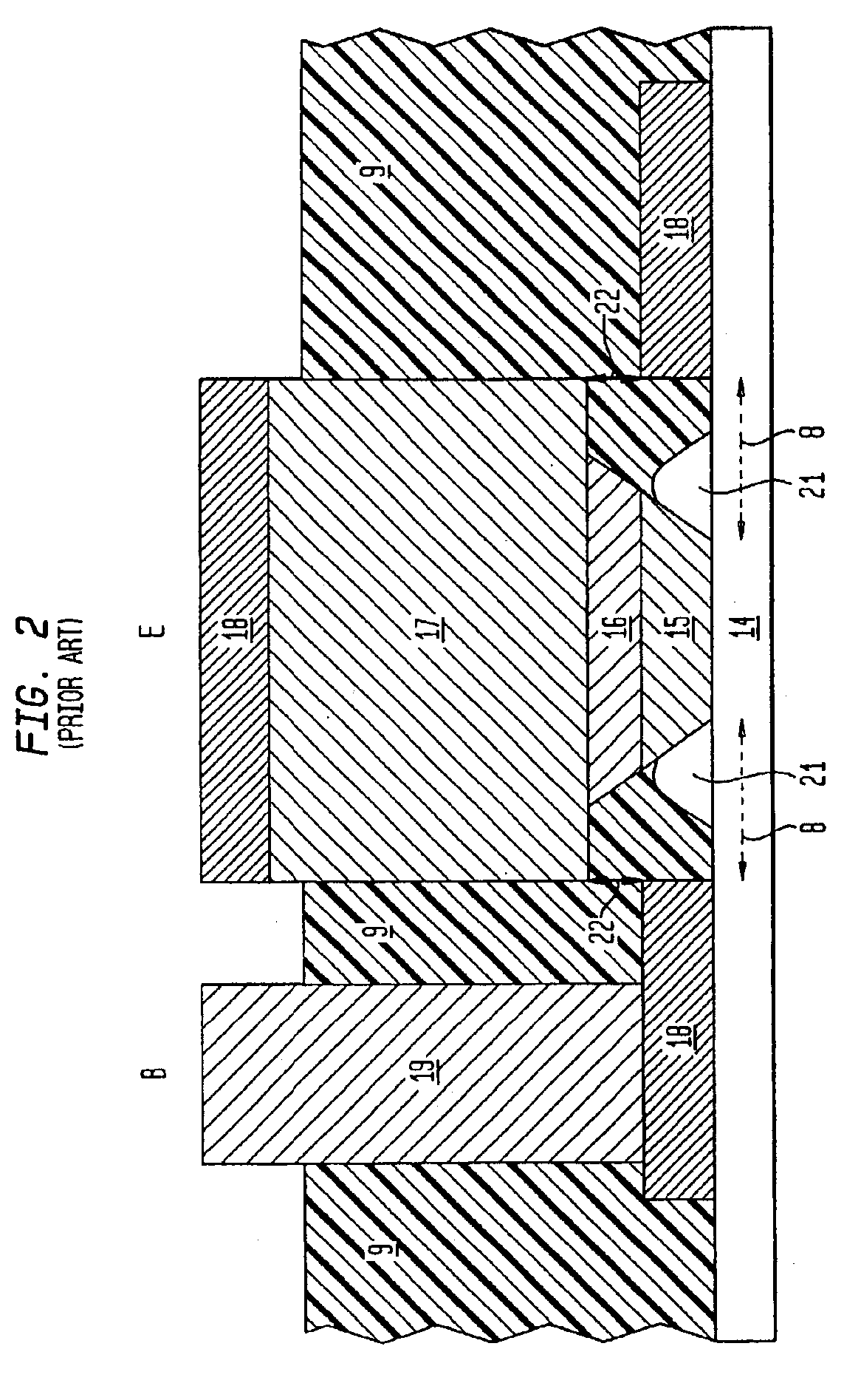
[0064]The present invention relates to the method of manufacturing a self-aligned HBT compound semiconductor using a dielectric-assisted metal lift-off process ...


PUM


Abstract

Disclosed is a manufacturing method to fabricate Heterojunction Bipolar Transistors (HBTs) that enables self-alignment of emitter and base metal contact layers with precise sub-micron spacing using a dielectric-assisted metal lift-off process. Such an HBT process relies on the formation of an “H-shaped” dielectric (i.e., Si3N4/SiO2) mask conformally deposited on top of the emitter contact metallization that is used to remove excess base metal through lift-off by a wet chemical HF-based etch. This HBT process also uses a thin selective etch-stop layer buried within the emitter layer to prevent wet chemical over-etching to the base and improves HBT reliability by forming a non-conducting, depleted ledge above the extrinsic base layer. The geometry of the self-aligned emitter and base metal contacts in the HBT insures conformal coverage of dielectric encapsulation films, preferably Si3N4 and/or SiO2, for reliable HBT emitter p-n junction passivation. Thus, the disclosed HBT process enables scaling of narrow emitter stripe widths down to sub-micron dimensions producing transistors with cut-off frequencies in the range of several hundred GigaHertz.

Description

CROSS-REFERENCE TO RELATED APPLICATIONS[0001]This application is a continuation of application Ser. No. 09 / 813,293, filed Mar. 20, 2001, which is now U.S. Pat. No. 6,541,346.TECHNICAL FIELD OF THE INVENTION[0002]The present invention relates to semiconductor transistors used in the fabrication of very high-speed integrated circuits and microwave power amplifiers. More particularly, the invention pertains to compound semiconductor transistors made from GaAs and InP and related lattice-matched materials epitaxially grown on semi-insulating substrates.BACKGROUND OF THE INVENTION[0003]Transistors are multielectrode semiconductor devices in which the current flowing between two specified electrodes is controlled or modulated by the voltage applied at a third (control) electrode. Transistors fall into two major classes: the bipolar junction transistor (BJT) and the field-effect transistor (FET). BJTs were derived from the point-contact transistor, which was invented at Bell Telephone Labo...

Claims


Application Information

Patent Timeline
IPC IPC(8): H01L21/331H01L21/02
CPCH01L29/66318H01L2224/0401H01L2224/06102H01L2224/1403H01L2924/1305H01L2924/00
Inventor MALIK, ROGER J.
Owner RJM SEMICON
Why Eureka
Try Eureka