Material for forming organic film, substrate for manufacturing semiconductor device, method for forming organic film, patterning process, and compound for forming organic film
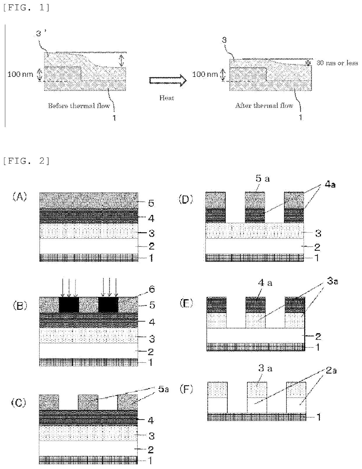
a technology of organic film and organic film, which is applied in the direction of photosensitive material processing, basic electric elements, electric instruments, etc., can solve the problems of pattern collapse, miniaturization of semiconductor device manufacturing process approaching the limit inherent in the wavelength of light source for photolithography, and substrate corrosion, etc., to prevent substrate corrosion, excellent and high filling and planarizing properties
- Summary
- Abstract
- Description
- Claims
- Application Information
AI Technical Summary
Benefits of technology
Problems solved by technology
Method used
Image

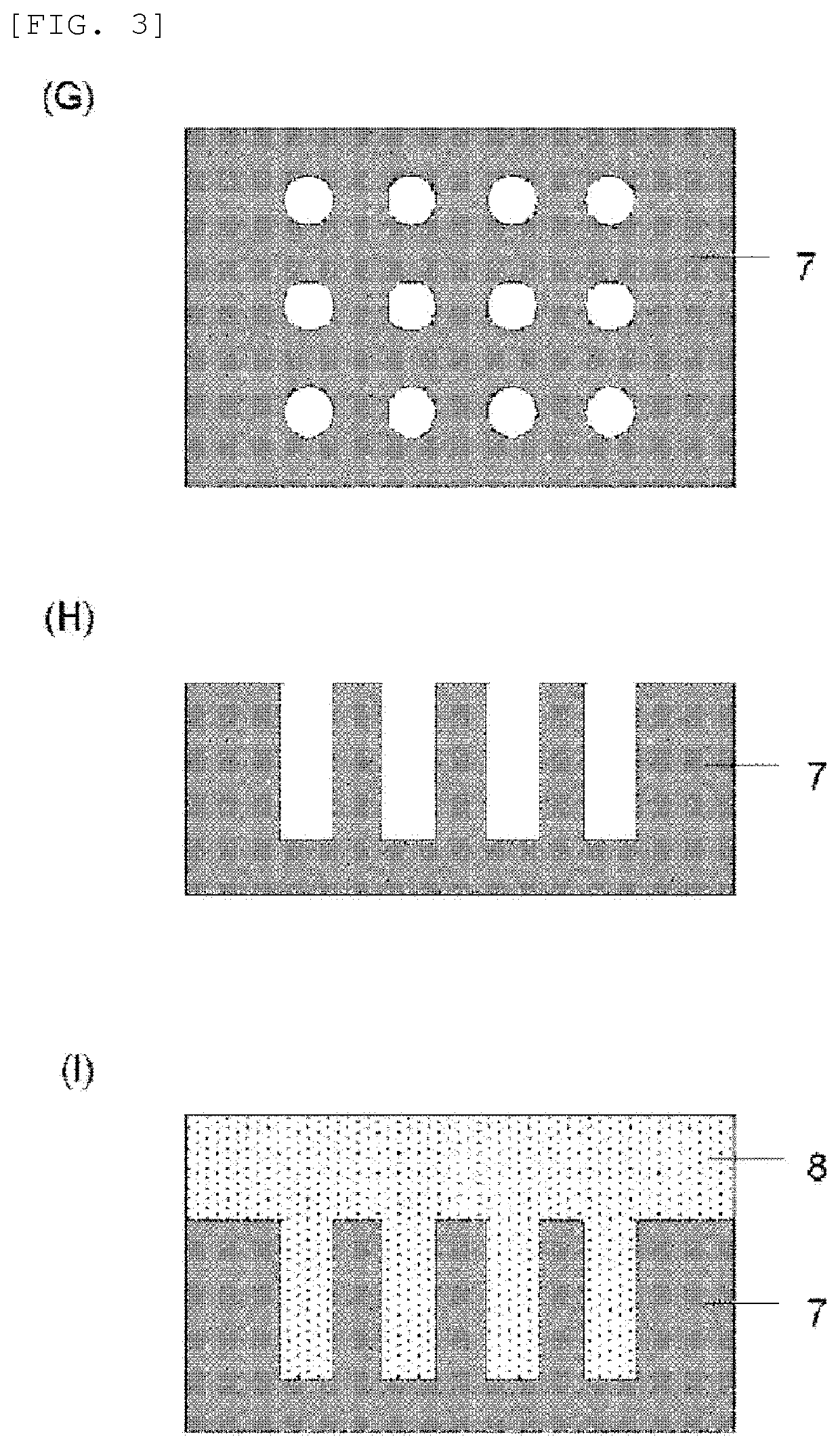
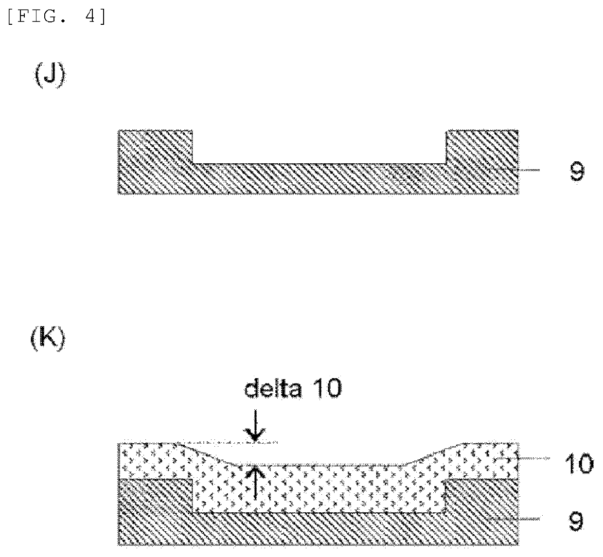
Examples
synthesis example 1
[Synthesis Example 1] Synthesis of Compound (A1)
[0263]120 g of NMP (N-methyl-2-pyrrolidone) was added to 7.91 g of amine compound (B1) and 17.21 g of phthalic anhydride derivative (C1), and under a nitrogen atmosphere, the reaction was allowed to proceed at an inner temperature of 40° C. for 3 hours to obtain an amic acid solution. 3.96 g of pyridine was added to the obtained amic acid solution, and 12.26 g of acetic anhydride was further added dropwise slowly. Then, the reaction was allowed to proceed at an inner temperature of 60° C. for 4 hours for imidization. After completion of the reaction, the solution was cooled to room temperature, 300 g of methyl isobutyl ketone was added, and the organic layer was washed with 100 g of 3% nitric acid aqueous solution. Then, the organic layer was further washed five times with 100 g of pure water and was evaporated under reduced pressure to dryness. To the residue, 100 g of THF (tetrahydrofuran) was added, and a homogeneous solution was fo...
synthesis example 14
[Synthesis Example 14] Synthesis of Compound (A14)
[0266]120 g of NMP was added to 15.98 g of amine compound (B11) and 10.33 g of phthalic anhydride derivative (C1), and under a nitrogen atmosphere, the reaction was allowed to proceed at an inner temperature of 40° C. for 3 hours to obtain an amic acid solution. After completion of the reaction, the solution was cooled to room temperature, 300 g of methyl isobutyl ketone was added, and the organic layer was washed with 100 g of 3% nitric acid aqueous solution. Then, the organic layer was further washed five times with 100 g of pure water and was evaporated under reduced pressure to dryness. To the residue, 100 g of THF was added, and a homogenous solution was formed. Thereafter, a crystal was precipitated in 300 g of hexane. The precipitated crystal was separated by filtration, washed twice with 200 g of hexane, and collected. The collected crystal was vacuum dried at 70° C. Thus, (A14) was obtained.
[0267]When the weight average mole...
synthesis example 15
[Synthesis Example 15] Synthesis of Compound (A15)
[0268]A homogeneous dispersion was formed from 10.00 g of the compound (A14), 4.16 g of potassium carbonate, and 50 g of NMP under a nitrogen atmosphere at an inner temperature of 50° C. 3.75 g of n-butyl bromide was slowly added dropwise, and the reaction was allowed to proceed at an inner temperature of 50° C. for 16 hours. After cooling to room temperature, 100 g of methyl isobutyl ketone and 50 g of pure water were added for homogenization, then, the aqueous layer was removed. Further, the organic layer was washed twice with 30 g of a 3.0% nitric acid aqueous solution and five times with 30 g of pure water. The organic layer was evaporated under reduced pressure to dryness. To the residue, 30 g of THF was added, and a crystal was precipitated with 100 g of methanol. The precipitated crystal was separated by filtration, washed twice with 60 g of methanol, and collected. The collected crystal was vacuum dried at 70° C. Thus, (A15) ...
PUM
| Property | Measurement | Unit |
|---|---|---|
| boiling point | aaaaa | aaaaa |
| temperature | aaaaa | aaaaa |
| temperature | aaaaa | aaaaa |
Abstract
Description
Claims
Application Information
 - R&D
- Intellectual Property
- Life Sciences
- Materials
- Tech Scout
- Unparalleled Data Quality
- Higher Quality Content
- 60% Fewer Hallucinations
Browse by: Latest US Patents, China's latest patents, Technical Efficacy Thesaurus, Application Domain, Technology Topic, Popular Technical Reports.
© 2025 PatSnap. All rights reserved.Legal|Privacy policy|Modern Slavery Act Transparency Statement|Sitemap|About US| Contact US: help@patsnap.com