
Method of fabricating free-form, high-aspect ratio components for high-current, high-speed microelectronics

a microelectronic and high-speed technology, applied in the field of three-dimensional microelectronic structures, can solve the problems of non-intuitive more complex structures may be created, and the creation of 3-d electronic components and devices is far greater

Inactive Publication Date: 2010-11-18
TRIAD NAT SECURITY LLC
View PDF2 Cites 1 Cited by
  • Summary
  • Abstract
  • Description
  • Claims
  • Application Information

AI Technical Summary

Benefits of technology

[0007]During FE-HP-LCVD an electrode, or array of electrodes, as described in patent application Ser. No. 11 / 143,179, filed Jun. 2, 2005 and incorporated herein by reference, may be used in opposition to the growing structures (fibers), with an applied voltage between the fibers and electrodes to generate a high-pressure discharge in the gases between the fiber(s) and electrode(s). Field- and thermionic-emission from the fiber tip(s) facilitate this discharge. This allows specific gas-phase species to be generated and accelerated onto the fiber tips, which can influence the composition and structure of the deposit material. This is important for the generation of particular electronic material properties, e.g. dopant states and levels.
[0009]The present invention describes a novel method of manufacturing complex three-dimensional (3-D) micro- and nano-scale (i.e., typically larger than 300 nm) electronic structures and components. The method of the present invention grows insulators, semiconductors, and metallic conductors to form standard semiconductor microcircuits and novel, complex 3-D microsystems composed of semiconductors, metallic connections, and pathways. The method of the present invention may be used to grow small semiconductor crystals and doped conductive lines in the complex patterns and associations required for 3-D microelectronics, and the post-processing necessary for device activation. This method results in devices with unprecedented performance compared with those produced by other standard lithographic methods, and allows for their vertical integration.
[0011]The method of the present invention may also allow miniaturization and integration of vacuum electronics, e.g., metallic conductors and waveguides for terahertz signals, and also micro-vacuum electronics devices such as micro-klystrons and micro-travelling wave tubes. These non-linear devices have many useful characteristics that are needed for communications, analog signal processing, power switching, and high speed computing. Through the process of the present invention, such devices can be integrated with semiconductor devices, and their reduced dimensions will allow low-voltage operation and ultra-high speed switching speeds (>1 THz), which ultimately could replace solid-state devices.
[0015]Hence, the process of the present invention performs the function of many traditionally separate processing steps as a single process, greatly reducing the number of processing steps and types of fabrication tools needed to create microelectronics. Although photolithographic methods excel at producing planar assemblies of integrated circuits, they usually require many mask exposures and process steps, often requiring realignment between steps. With the present process, however, device materials are essentially “auto-aligned” as they are grown, eliminating most of the alignment steps commonly required with lithographic processing. In addition, the number of discrete processes is greatly reduced; no longer are DUV steppers, pattern generators, spin coaters, reactive ion etchers, ion implanters, low-pressure CVD coaters, PVD coaters, wire bonders, etc. all required to fabricate and interconnect devices. The present process reduces the cost of microelectronics prototyping and fabrication by over 85%, where traditional ICs are not required.
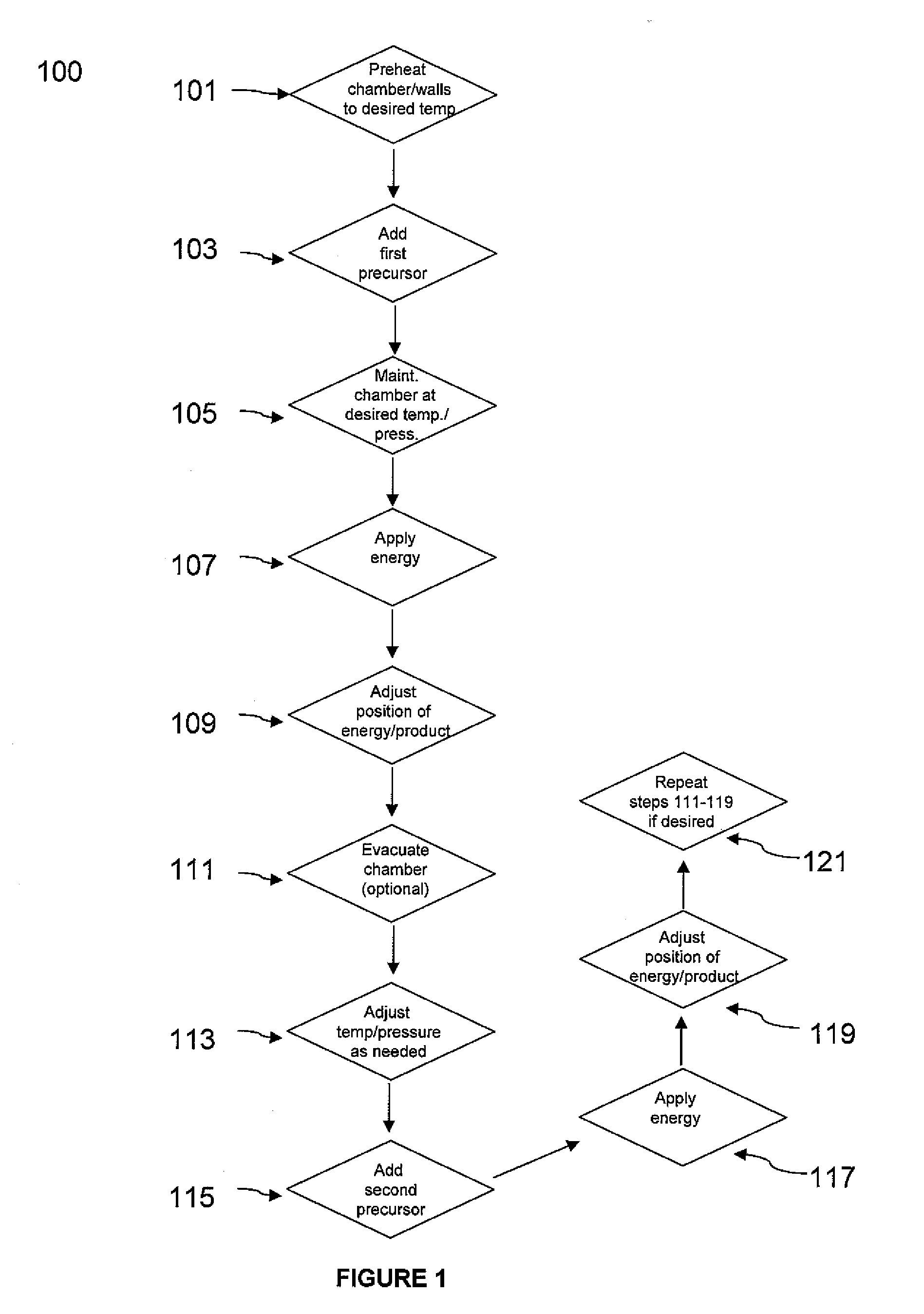
[0017]According to a first embodiment of the present invention, a method of fabricating a three-dimensional microelectronic structure is provided, comprising passing a first precursor material for a selected three-dimensional microelectronic structure into a reaction chamber at temperatures sufficient to maintain said precursor material in a predominantly gaseous state; maintaining said reaction chamber under sufficient pressures to enhance formation of a first portion of said three-dimensional microelectronic structure; applying an electric field between an electrode and said microelectronic structure at a desired point under conditions whereat said first portion of a selected three-dimensional microelectronic structure is formed from said first precursor material; positionally adjusting either said formed three-dimensional microelectronic structure or said electrode whereby further controlled growth of said three-dimensional microelectronic structure occurs; passing a second precursor material for a selected three-dimensional microelectronic structure into a reaction chamber at temperatures sufficient to maintain said precursor material in a predominantly gaseous state; maintaining said reaction chamber under sufficient pressures whereby a second portion of said three-dimensional microelectronic structure formation is enhanced; applying an electric field between an electrode and said microelectronic structure at a desired point under conditions whereat said second portion of a selected three-dimensional microelectronic structure is formed from said second precursor material; and, positionally adjusting either said formed three-dimensional microelectronic structure or said electrode whereby further controlled growth of said three-dimensional microelectronic structure occurs.

Problems solved by technology

More complex structures also may be created by continuously reorienting and scanning the electrode.
However, the creation of 3-D electronic components and devices presents far greater challenges and is non-intuitive.

Method used


Image

  • Method of fabricating free-form, high-aspect ratio components for high-current, high-speed microelectronics
  • Method of fabricating free-form, high-aspect ratio components for high-current, high-speed microelectronics
  • Method of fabricating free-form, high-aspect ratio components for high-current, high-speed microelectronics

Examples


example 1

Tungsten Fibers

[0067]Several dozen pure tungsten fibers were grown using WF6+H2 or WCI6+H2 gas mixtures. WF6+H2 proved to be the superior precursor system for both growth rates and lack of deposit impurities. Even at hyperbaric pressures, the kinetics of WCI6+H2 deposition was very slow. Using WF6+H2, very rapid steady-state growth rates were obtained, ranging from 3-160 μm / s. Typical gas mixtures were 3:1 H2 to WF6, and a cw Ar+laser was used at laser powers from 400 mW to 12 W. The purity of the deposit was examined by energy dispersive X-ray spectroscopy (EDS) and Auger spectroscopy. Essentially no trace of fluorine was detected in the deposits, and only a thin native oxide was present, due to exposure to air prior to characterization. The microstructures of the fibers varied greatly, depending on the precursor pressures and laser powers employed. At WF6 partial pressures of 350 mbar and laser powers of 800-900 mW, the fine tungsten fibers grew as highly-oriented single-crystals ...

example 2

Schottky Diode

[0068]A three-dimensional Shottky diode was fabricated as follows. An indium-doped silicon fiber was grown using as precursors materials for indium trimethylindium ((CH3)3In) and cyclopentadienylindium (C5H5In) and as precursor materials for silicon silane (SiH4) and disilane (Si2H6). To achieve sufficient conductivity of the silicon single-crystals, the concentration of indium precursors in the gas phase may be less than 1000 ppm. The chamber pressure ranged from 600-1200 torr, and a cw Nd:YAG laser was used at laser powers from 200 mW to 3 W. An electrode also could be used to impart comparable energy, as would be understood by one of skill in the art.

[0069]The quantity of indium was slowly decreased, while adding very small quantities of boron (<1 torr) by means of a boron precursor. Suitable boron precursors include among others diborane, trimethylboron, triethylboron, triphenylboron, and decaborane. The slow addition of boron creates a boron-doped section in the s...

example 3

[0073]A hybrid three-dimensional micromechanical spring assembly, electrical coil, and electrodes were fabricated as follows: A supporting fiber was grown of carbon from ethylene. A soft mechanical spring was created of hydrogenated diamond-like carbon from ethylene and hydrogen. The growth rates were 15-20 microns per second, and the laser power was approximately 300-400 mW. Probes and coils were fabricated of carbon and tipped / coated with proprietary metals. This assembly was only 2-3 mm long, and functioned as a rudimentary accelerometer that responds to frequencies down to about 25 Hz.

[0074]In all embodiments of the present invention, all percentages are by weight of the total composition, unless specifically stated otherwise. All ratios are weight ratios, unless specifically stated otherwise. All ranges are inclusive and combinable. The number of significant digits conveys neither a limitation on the indicated amounts nor on the accuracy of the measurements. All numerical amoun...


PUM


Abstract

Microelectronic structures and devices, and method of fabricating a three-dimensional microelectronic structure is provided, comprising passing a first precursor material for a selected three-dimensional microelectronic structure into a reaction chamber at temperatures sufficient to maintain said precursor material in a predominantly gaseous state; maintaining said reaction chamber under sufficient pressures to enhance formation of a first portion of said three-dimensional microelectronic structure; applying an electric field between an electrode and said microelectronic structure at a desired point under conditions whereat said first portion of a selected three-dimensional microelectronic structure is formed from said first precursor material; positionally adjusting either said formed three-dimensional microelectronic structure or said electrode whereby further controlled growth of said three-dimensional microelectronic structure occurs; passing a second precursor material for a selected three-dimensional microelectronic structure into a reaction chamber at temperatures sufficient to maintain said precursor material in a predominantly gaseous state; maintaining said reaction chamber under sufficient pressures whereby a second portion of said three-dimensional microelectronic structure formation is enhanced; applying an electric field between an electrode and said microelectronic structure at a desired point under conditions whereat said second portion of a selected three-dimensional microelectronic structure is formed from said second precursor material; and, positionally adjusting either said formed three-dimensional microelectronic structure or said electrode whereby further controlled growth of said three-dimensional microelectronic structure occurs.

Description

CROSS REFERENCE TO RELATED APPLICATION[0001]This application claims the benefit of priority of U.S. Provisional Patent Application 61 / 211,839, filed Apr. 3, 2009, and incorporated herein in its entirety.STATEMENT REGARDING FEDERAL RIGHTS[0002]This invention was made with government support under Contract No. DE-AC 52-06NA25396, awarded by the U.S. Department of Energy. The government has certain rights in the invention.FIELD OF THE INVENTION[0003]The invention relates to three-dimensional microelectronic structures and processes for growth thereof employing field emission laser chemical vapor deposition (FE-LCVD) and field emission high pressure (hyperbaric) laser chemical vapor deposition (FE-HP-LCVD).BACKGROUND OF THE INVENTION[0004]Microelectronic fabrication technology is an extremely diverse field, ranging from the fabrication of discrete custom-made components to on-chip digital / analog circuits with their associated higher-level packaging. However, most of the devices that for...

Claims


Application Information

Patent Timeline
IPC IPC(8): H01L21/205H01L21/02H01L29/861
CPCB81C1/0019H01L21/02521H01L21/02532H01L21/02573H01L21/0259H01L29/872H01L21/02636H01L21/28556H01L21/8213H01L29/66143H01L21/0262
Inventor MAXWELL, JAMES L.ROSE, CHRIS R.BLACK, MARCIE R.SPRINGER, ROBERT W.
Owner TRIAD NAT SECURITY LLC
Learn More