
Copper/niobium composite piping material produced by copper electroforming, process for producing the same and superconducting, acceleration cavity produced from the composite piping material

Inactive Publication Date: 2010-03-18
HIGH ENERGY ACCELERATOR RESEARCH ORGANIZATION +1
View PDF5 Cites 11 Cited by
  • Summary
  • Abstract
  • Description
  • Claims
  • Application Information

AI Technical Summary

Benefits of technology

[0014]As described above, the conventional processes for producing a superconducting acceleration cavity and acceleration cavities produced thereby have many problems. Therefore, in this field, the followings have been desired: (1) electron beam welded sites are decreased up to a limit, and producing costs and welding defects are largely reduced; (2) defects resulting from weld lines present in the circumferential direction (the equator portionial direction) of a cavity are removed, so that a quench phenomenon based on local generation of heat is avoided to attain a high accelerating electric field; and (3) the amount used of expensive niobium material is decreased, and a local heat-generation phenomenon originating from a high resistance of niobium material is suppressed, thereby attaining a high accelerating electric field at low costs.
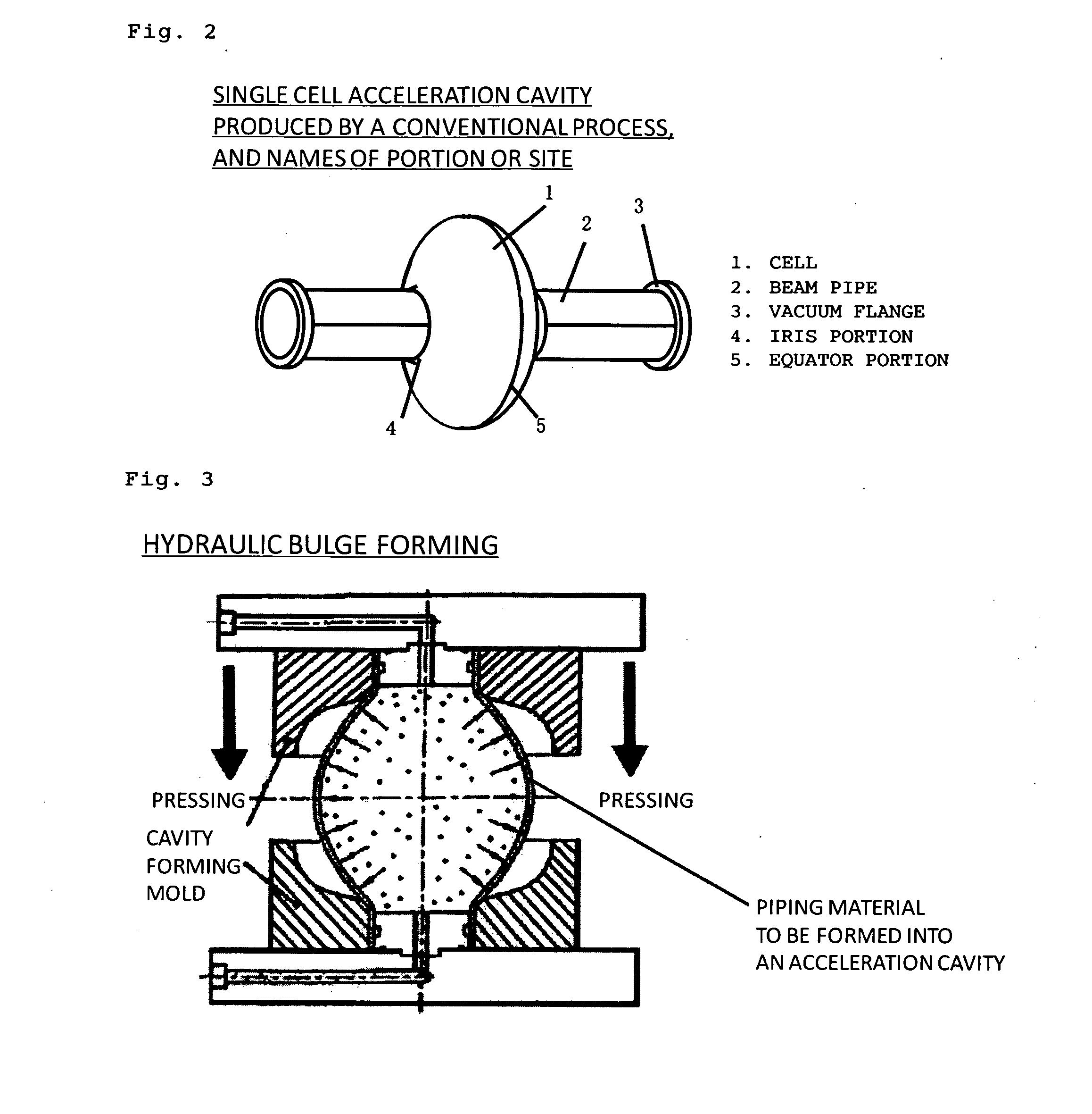
[0016]The present inventors have considered trying to provide a novel composite seamless piping material which is made of copper and niobium and has a large bonding strength permitting the material to resist against hydraulic bulge forming, thereby embodying an acceleration cavity which can simultaneously attain low costs and a high accelerating electric field. For more detail, the present inventors have considered trying to use a niobium piping material prepared in advance, adopt a widely-usable electroforming process without using special producing facilities to embody a strong adhesiveness between electroformed copper and niobium which has not been attained up to now and produce a novel electroformed copper / niobium composite piping material which can permit a high working stress at the time of hydraulic bulge forming and an extensibility at the time of enlarging the pipe. The principle of hydraulic bulge forming is shown in FIG. 3.
[0032]In other words, the present invention relates to essentially a process for coating a niobium piping material with copper; thus, it does not become necessary at all to care about the fitting precision between a copper pipe and a niobium pipe as when the process of JP-A-2000-306697 described above is carried out. After an electroformed copper layer is formed, copper and niobium are present closely to each other, which is most ideal for HIP bonding method. In this case, when the electroformed copper layer is formed, copper electroforming coating should be performed with anodes arranged on the inner and outer surfaces of the niobium piping material in order to avoid a deterioration of niobium at high temperature and high pressure, which is a drawback of HIP bonding method. However, an excess of copper on the inner surface must be finally removed with nitric acid or the like. This generates futility. However, when HIP bonding method is applied to an electroformed copper / niobium piping material, there are generated advantages that the piping material is released from a problem about the dimensional precision for fitting a copper piping material and a niobium piping material to each other and a restriction of the length thereof.
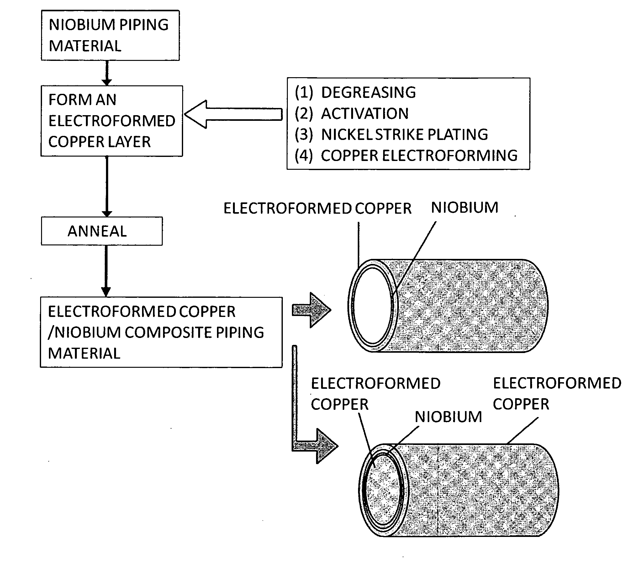
[0052]According to the producing process of the present invention, an electroformed copper / niobium composite piping material, in particular, a composite piping material wherein no or few seams are present can be industrially advantageously produced. Moreover, in the electroformed copper / niobium composite piping material of the present invention, a niobium piping material and electroformed copper are bonded to each other with a nickel thin film interposed therebetween; therefore, the adhesiveness between the electroformed copper and the niobium thin piping material is high, and the composite piping material can resist sufficiently against pipe-enlargement based on hydraulic bulge forming. Accordingly, the present invention is in particular useful for the material of a superconducting acceleration cavity.

Problems solved by technology

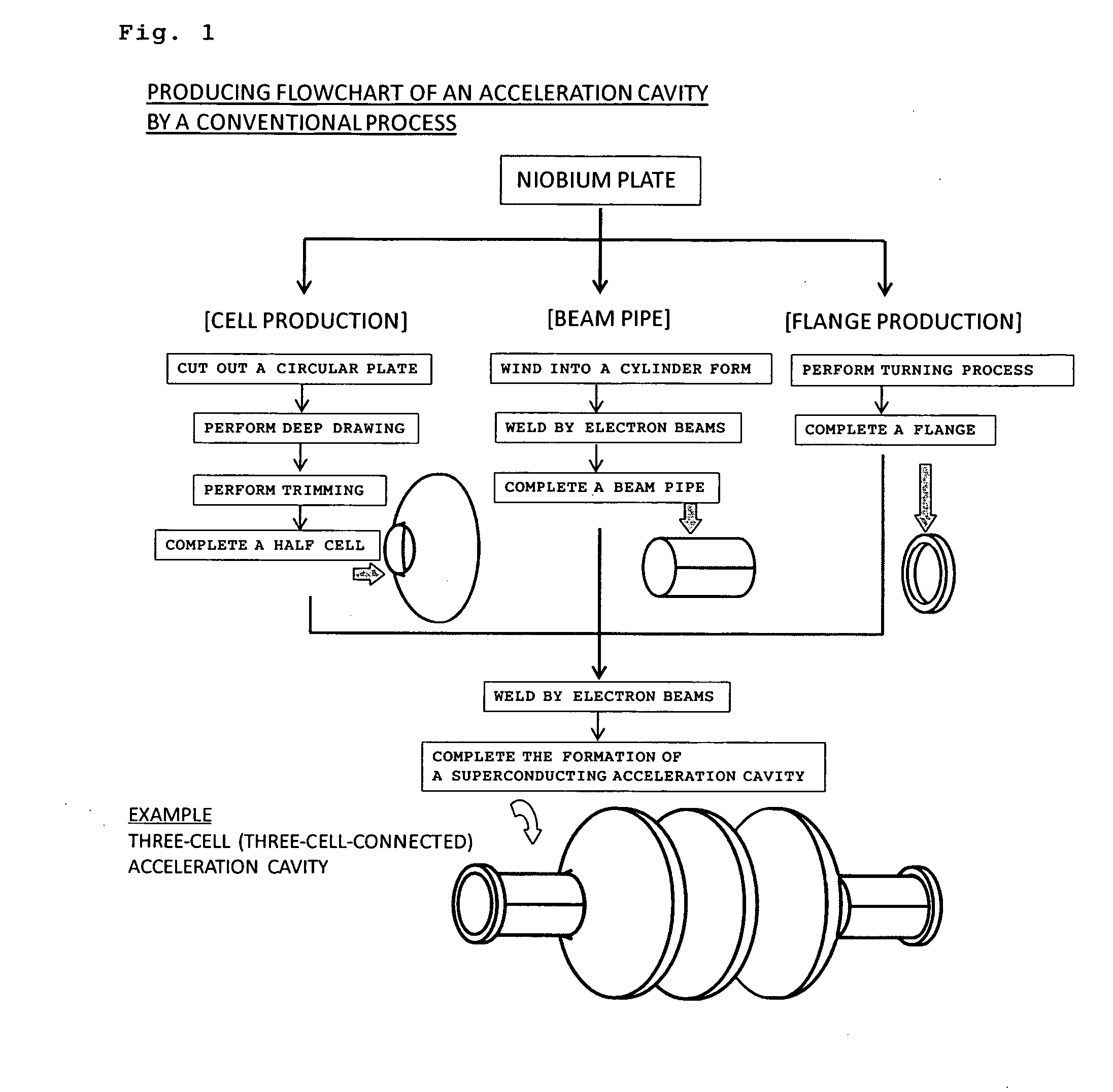
This production process requires many working steps; thus, there exists a problem that costs for producing an acceleration cavity are inevitably increased up.
Furthermore, there exists a basic problem concerned with accelerating performances since electron beam welding is frequently used.
For example, when welding defects are present, in particular, such defects are present in the equator portion of a cavity, heat is often generated in welded sites.
However, in this process, no considerations are made for pollution of the niobium surface generated at the time of removing the aluminum or the alloy thereof with an acid or alkali, the purity of the formed niobium film, and stress to which the niobium thin film is subjected by the pipe-enlarging working.
Thus, the process is a process which cannot be practically used at all.
Additionally, there are problems about costs such that an expensive large-sized vacuum film-forming apparatus for forming a niobium thin film and a copper thin film is indispensable.
However, the acceleration cavity itself originally has a spherical form, so that there is caused a problem about the evenness of the film thickness distribution of the niobium thin film obtained by sputtering.
There is also caused a basic problem which affects performances, an example thereof being pinholes which are frequently encountered in the form of thin films.
Furthermore, as well as the process of JP-A-60-261202, there has not yet been overcome a problem of the dissolution of niobium or the reduction in the thickness of niobium which follows chemical polishing or electropolishing of the inner surface of the cavity for the purpose of removing the surface pollution of the inside of the cavity.
If the film thickness is made large under consideration of dissolution loss of the niobium by the chemical polishing or the electropolishing, there are caused not only a problem about the time for forming the film but also a problem about the flatness of the surface.
Moreover, as well as the case of JP-A-60-261202, a large-sized and expensive vacuum film-forming apparatus is essential.
Accordingly, the production process of JP-A-1-231300 cannot be a stable process for producing a superconducting acceleration cavity since the process has many practical evil effects and cannot give a high accelerating electric field from the viewpoint of performances.
However, supplementary experiments by the present inventors have demonstrated that the formation of a diffusion layer of gold onto niobium is not observed at the above-mentioned temperature, and no effect of improving the adhesiveness is found out.
Furthermore, it is technically impossible for copper electroplating or copper spraying to assure an even film thickness on the outer peripheral surface of a superconducting acceleration cavity which is largely undulating in the shape thereof.
Thus, it is doubtful that the process will be realized.
Additionally, the process is involved in a serious problem that specific sites are cracked; thus, the process is not a useful process.
As a result, the following problems are not overcome: a problem that niobium material, which is expensive, is used in a thick wall form; and a problem that a high electric resistance of niobium at normal temperature induces a local heat generation phenomenon (called a hot spot), which hinders a highly accelerating electric field at very low temperatures, to cause the quench of the superconductive state.
Niobium material essentially has these problems.
However, there remains a problem that after the end of the bulge forming, the copper piping material of the inner cylinder must be dissolved and removed with a chemical agent for dissolving copper, for example, nitric acid.
Additionally, the HIP bonding method itself requires an expensive and special apparatus and further the method is basically batch working.
Furthermore, the most serious problem when the HIP bonding method is applied to the production of the above-mentioned copper / niobium composite pipe is that when the inner cylinder, the niobium pipe and the outer cylinder are designed and formed in such a manner that the fitting crossing of the diameters can have a margin so as to attain the insertion of each of the cylinders and the pipe with ease, the bonding strength cannot be sufficiently kept.
Accordingly, apart from the case of forming a composite piping material for a superconducting acceleration cavity having a short length in the axial direction, the HIP bonding is unsuitable for the process for producing a composite piping material for an ordinary superconducting cavity having a total length of 1 m or more.
However, this process is too complicated.
Thus, apart from the case of carrying out mass production of clad element pipes, the process is unsuitable for the aim of lowering costs.

Method used


Image

  • Copper/niobium composite piping material produced by copper electroforming, process for producing the same and superconducting, acceleration cavity produced from the composite piping material
  • Copper/niobium composite piping material produced by copper electroforming, process for producing the same and superconducting, acceleration cavity produced from the composite piping material
  • Copper/niobium composite piping material produced by copper electroforming, process for producing the same and superconducting, acceleration cavity produced from the composite piping material

Examples


example 1

[0078]A niobium plate of 1.0 mm thickness, 500 mm length and 400 mm width was subjected to a plate-winding process, and the joint was subjected to electron beam welding (EBW) to form a niobium piping material of 127 mm diameter and 500 mm length. The surface of the niobium piping material was subjected to wet polishing finishing with a #400 emery paper. Thereafter, an electrolytic degreasing solution, an electrolytic activating solution and a nickel strike plating solution and applied conditions described in below Table 6 were used to conduct cathodically electrolytic degreasing treatment and cathodically electrolytic activating treatment. Then, the resultant was coated with nickel strike plating. Next, under conditions that the concentration of copper sulfate, that of sulfuric acid and that of chlorine ion were 152 g / L, 135 g / L and 20 mg / L, respectively, the temperature was 25° C. and a current density was 3 A / dm2, the niobium thin piping material was coated with electroformed copp...


PUM

PropertyMeasurementUnit
Temperatureaaaaaaaaaa
Lengthaaaaaaaaaa
Lengthaaaaaaaaaa

Abstract

In order to produce industrially advantageously an electroformed copper / niobium composite piping material wherein an electroformed copper layer and a niobium thin piping material are strongly bonded to each other, the electroformed copper / niobium composite piping material can be produced by coating any one or each of the outer peripheral surface and the inner peripheral surface of a niobium thin piping material with a nickel thin film, coating the surface of the nickel thin film with copper by electroforming, and subsequently annealing the resultant.

Description

TECHNICAL FIELD[0001]This invention relates to a novel composite piping material which comprises electroformed copper and niobium integrated and bonded strongly with each other, and which can be a starting material for producing a superconducting acceleration cavity that does not have basically any continuous seams by welding along the circumferential direction thereof; a process for producing the same; a superconducting acceleration cavity formed from the composite piping material; and a process for producing the same.BACKGROUND ART[0002]Conventionally, a process that has been most ordinarily adopted as a process for producing a superconducting acceleration cavity for accelerating charged particles such as electrons, positrons or protons at high frequencies is a process of selecting deep drawing, cutting or some other working appropriately to form plate-form niobium into main parts which constitute a cavity, and then bonding and integrating these with each other by electron beam we...

Claims


Application Information

Patent Timeline
IPC IPC(8): C25D5/28C25D7/04C25D5/12C25D5/50B21C37/06H05H7/20
CPCB21C37/06B21C37/16B21D15/10C25D1/02Y10T428/12292C25D5/12C25D5/50C25D7/04H05H7/20C25D3/38
Inventor SAITO, KENJIIKEDA, TOKUMIHIGUCHI, TAMAO
Owner HIGH ENERGY ACCELERATOR RESEARCH ORGANIZATION
Learn More