Complex oxides for use in semiconductor devices and related methods

Inactive Publication Date: 2006-07-20
PENN STATE RES FOUND +1
View PDF12 Cites 129 Cited by
  • Summary
  • Abstract
  • Description
  • Claims
  • Application Information

AI Technical Summary

Benefits of technology

[0018] The first oxide layer can include a nitrided silicon dioxide and/or may contribute less than about 0.5 nm of oxide-equivalent capacitance to said field effect trans

Problems solved by technology

However, reduced EOT dielectrics may exhibit tunneling and current leakage.
However, dielectric materials with higher vales of K generally tend to have relatively small band gaps, which can also contribute to undesirable tunneling leakage current in semiconductor devices despite a relatively high dielectric constant.
These materials may not demonstrate the targeted goals of capacitance with decreased tunneling or leakage currents that may be desirable for silicon CMOS devices.
The performance of the materials may be limited due to the oxidation of the silicon substrate that can occur during thermal chemical vapor deposition (CVD) or during post-deposition processing, such as, for example, thermal anneals, to fully oxidize the deposited thin films.
Due to these properties, several high-K thin film dielectrics, including TiO2, Nb2O3 and Ta2O3 may perform poorly if incorporated into silicon MOSFET devices.
There may be other problems in the application of elemental oxides, such as the transition metal oxides, ZrO2, HfO2, Y2O3, La2O3, and the rare earth oxides (including Gd2O3 and the like), into aggressively scale miniaturized MOSFET devices.
The various problems that can be experienced include i) high values of interfacial fixed charge that are generally positive ii) ion and atom transport, iii) high reactivity with ambient gases, giving rise to incorporation or water or hydroxyl groups, and iv) lower than anticipated tunneling currents due to reduced electron masses associated with the electronic structure, e.g., because the lowest conduction band has d-state properties.
Other process integration issues may relate to the combined effects of their hydrophyllic nature and oxygen ion transport that can promote changes in interface bonding during post-deposition thermal process steps, including dopant activation of atoms in source and drain contacts to the channel in a MOSFET device.
However, one drawback for both group IVB silicates may be their thermal stability against chemical phase separation into ZrO2 or HfO2, and a relatively low content silicate alloy (less than 10% ZrO2 or HfO2 as determined by the concentration of the eutectic in the equilibrium phase diagram), and crystallization of the ZrO2 or HfO2 phase.
The separated state is lower in energy, but also has a significantly reduced dielectric constant that renders phase separated dielectrics not useful for certain applications.
In addition, the rigidity of these low ZrO2 / HfO2 content silicate films may result in i) defects in the bulk of the film that cannot be compensated by hydrogen or deuterium, and leads to electron injection and trapping under biased conditions, and also ii) defect formation at the semiconductor dielectric interfaces, e.g., silicon atom dangling bonds in the strained silicon in contact with the dielectric film, and / or a superficially thin region with predominantly Si—O bonding.
Other potential problems encountered with various high-K dielectrics may relate to: (1) the crystallization of the deposited films during either deposition or post-deposition processing, (2) the low dielectric constants of the bulk films that may be insufficient to meet the targeted goals, and (3) the formation of interfacial silicon oxides, or low content silicon oxide alloys (e.g., silicates) that may limit the attainable effective values of the K for the resulting stacked dielectric structure.
The formation of interfacial silicide bonds may result in undesirable interfacial defects.
Such defects may occur in the form of fixed positive charge or interface traps.
Utilizing such interfacial layers with known insulating film dielectrics, however, may be disadvantageous in that they may limit the dielectric stacks from having sufficient capacitance to meet the ever-increasing scaling demands of CMOS devices.
Additionally, this use of interfacial layers may also limit the incorporation of high-K oxides into devices that employ semiconductor substrates other than silicon such as, for example, silicon carbide, gallium nitride and compound semiconductors such as SiC, GaN, (Al,Ga)N, GaAs, (Al,Ga)As, (In,Ga)As, GaSb, (Al,Ga)Sb, (In,Ga)Sb, as well as nitride, arsenide and antimonide quaternary III-V alloys.

Method used


Image

  • Complex oxides for use in semiconductor devices and related methods
  • Complex oxides for use in semiconductor devices and related methods
  • Complex oxides for use in semiconductor devices and related methods

Examples


example 1

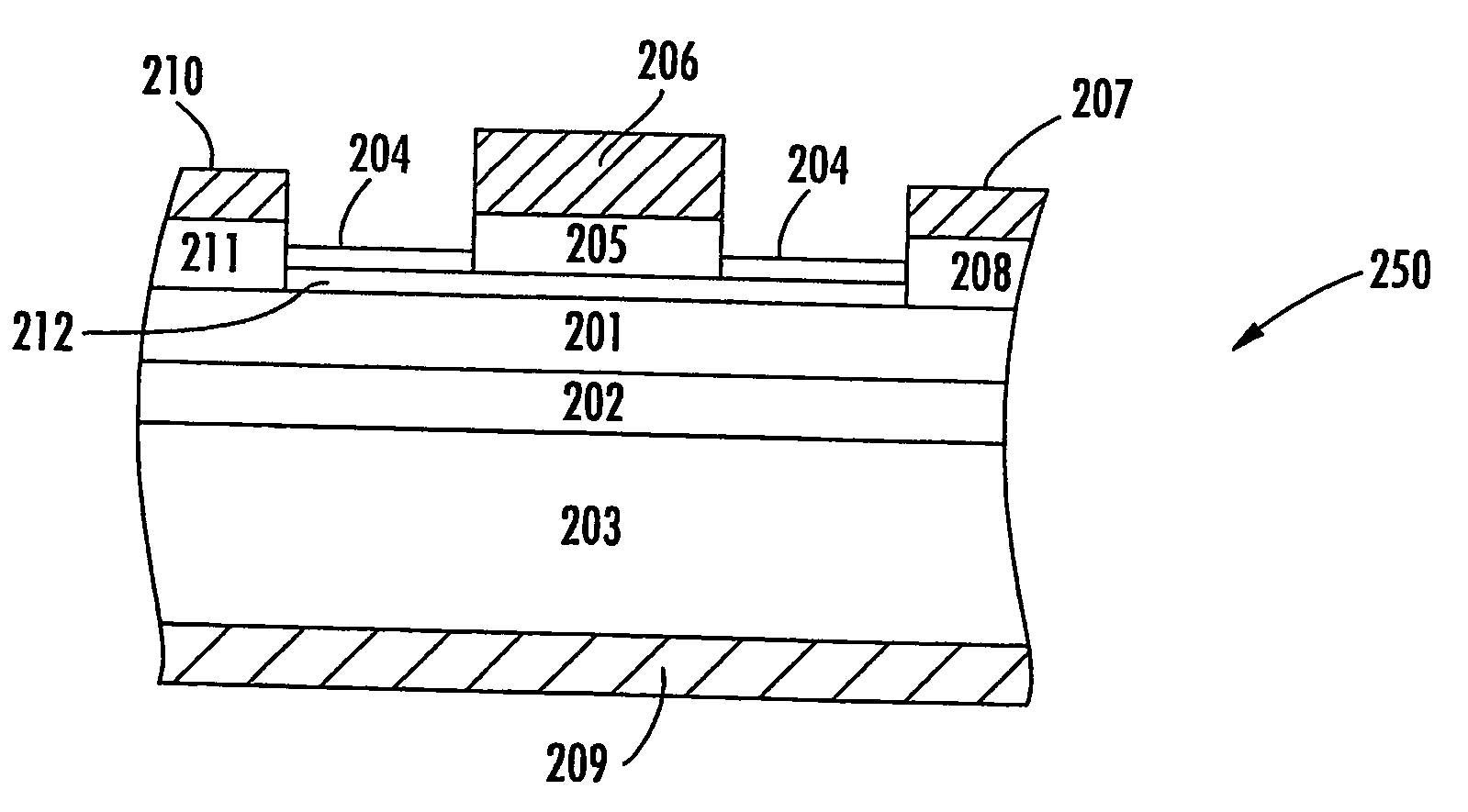
[0084] A field effect transistor is formed according to the following procedure. Radio frequency remote plasma assisted oxidation using oxygen as the source gas is employed to form an SiO2 insulating layer on a Si-containing substrate such as Si, SiC or a (Si,Ge) alloy. The above process is carried out at 300° C. A thin film, stoichiometric, single-phase complex oxide according to formula (I) is formed on the insulating layer via a radio frequency remote plasma enhanced CVD deposition carried out at 300° C. The structure is then exposed to a post deposition rapid thermal anneal in an inert, non-oxidizing ambient such as helium or argon for e.g., 30 seconds at 900° C.

[0085] The resulting field effect transistor has an SiO2 insulating layer with a thickness of less than 0.5 nm (i.e., 5 Å) and a gate insulating layer physical thickness of more than 2.0 nm (i.e., 20 Å), that, in combination with the interfacial SiO2 layer is chosen to meet the targeted EOT, e.g., in the range of 0.7 nm...

example 2

[0086] A field effect transistor is formed according to the procedure set forth in Example 1 with the following modifications. The substrate is exposed to an N2 remote plasma to allow for the formation of silicon-nitrogen bonding at the surface of the silicon substrate. The other layers are formed in the manner previously described.

example 3

[0087] A field effect transistor is formed according to the procedure set forth in Example 1 with the following modifications. A remote plasma assisted oxidation using N2O instead of O2 is employed to form a thin SiO2 layer with silicon-nitrogen boding at the silicon substrate.


PUM


Abstract

A semiconductor device includes a semiconductor substrate, a first oxide layer on the semiconductor substrate including an element from the semiconductor substrate, and a second oxide layer on the first oxide layer opposite the semiconductor substrate. The second oxide layer includes a stoichiometric, single-phase complex oxide represented by the formula: AhBjOk, or equivalently (AmOn)a(BqOr)b in which the elemental oxide components, (AmOn) and (BqOr) are combined so that h=j or, equivalently, ma=bq, and a, b, h, j, k, m, n, q and r are non-zero integers; and wherein: A is an element of the lanthanide rare earth elements of the periodic table or the trivalent elements from cerium to lutetium; and B is an element of the transition metal elements of groups IIIB, IVB or VB of the periodic table.

Description

FIELD OF THE INVENTION [0001] The invention generally relates to oxides that may be used in conjunction with integrated circuit devices, e.g., field effect transistors and high electron mobility transistors, as well as other devices including photovoltaics, and methods of making the same. BACKGROUND OF THE INVENTION [0002] Insulated gate field effect transistors (IGFETs) typically include a channel region in which current is controlled through the application of an electrical bias to a gate electrode that is separated from the channel region by a thin insulating film or gate dielectric. Current through the channel is supplied and collected by source and drain contacts, respectively, to the channel region. As semiconductor devices become increasingly miniaturized, gate dielectrics having a reduced equivalent oxide thickness (EOT) may be desirable. For example, the Semiconductor Industry Association (SIA) National Technology Roadmap for Semiconductors (NTRS) has projected that gate di...

Claims


Application Information

Patent Timeline
IPC IPC(8): H01L31/0328H01L21/336H01LH01L21/28H01L29/20H01L29/51H01L29/778H01L31/0216
CPCH01L21/28194H01L21/28202H01L21/3143H01L21/31604H01L29/2003H01L29/4908H01L29/513H01L29/517H01L29/7786H01L29/78H01L31/02161H01L21/02252H01L21/0214H01L21/02164H01L21/02192H01L21/02156H01L21/02238H01L21/02274H01L21/02178H01L21/0228
Inventor LUCOVSKY, GERALDSCHLOM, DARRELL
Owner PENN STATE RES FOUND
Why Eureka
Try Eureka