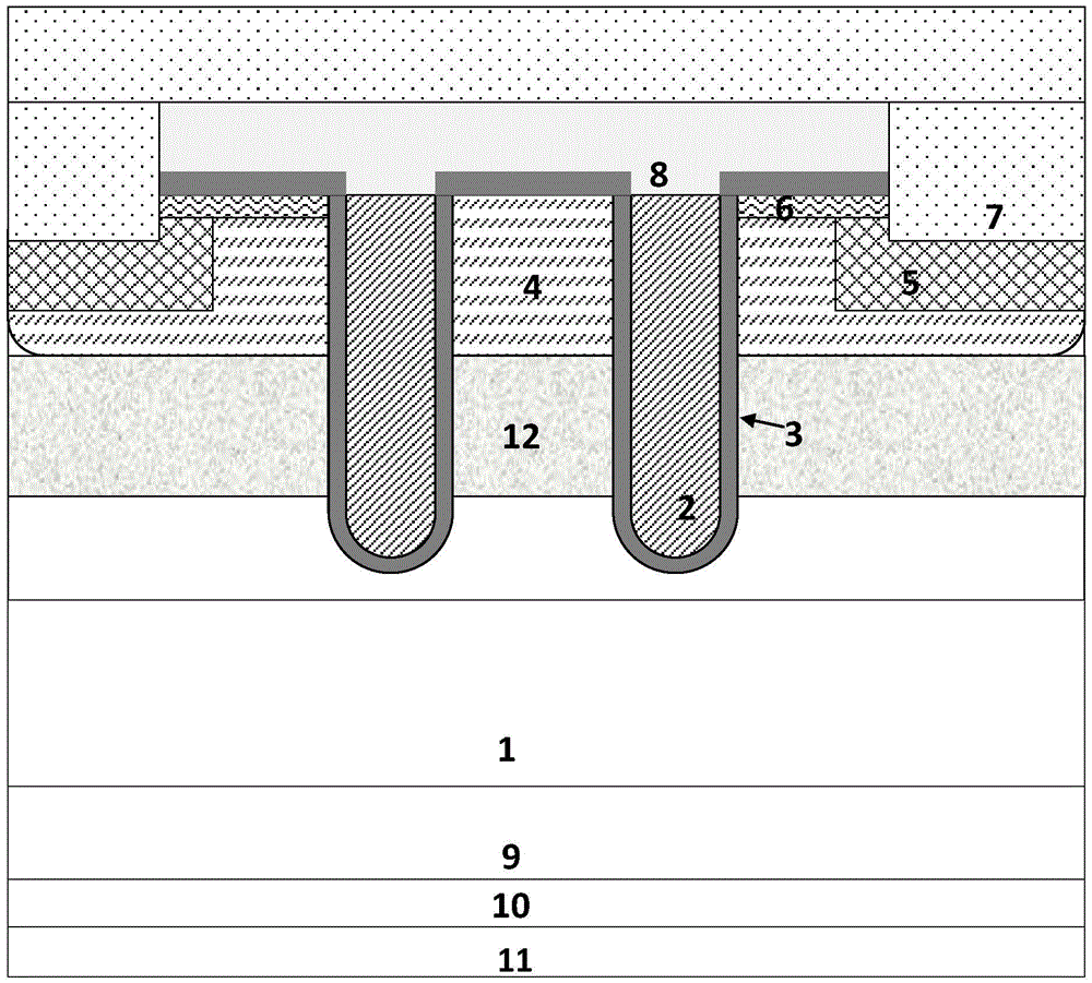
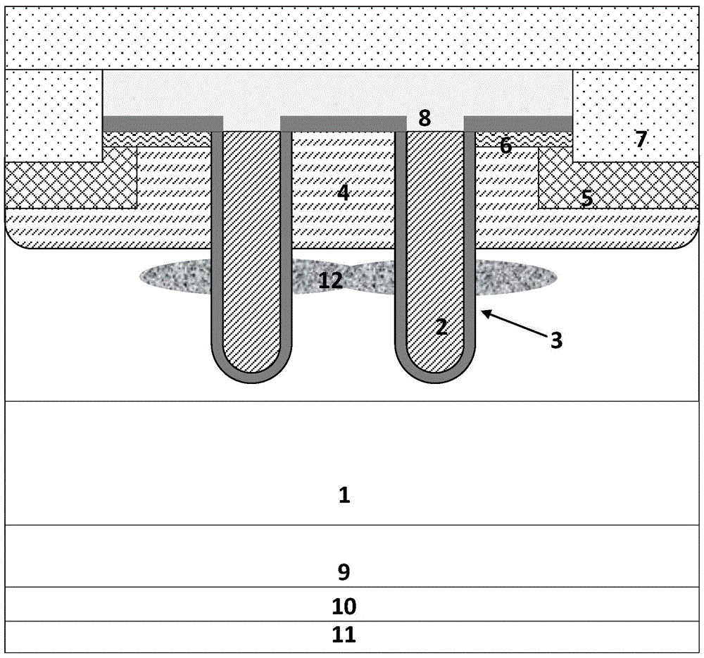
Method for forming IGBT (insulated gate bipolar transistor) charge storage layer and charge storage type IGBT
A technology of charge storage layer and oxide layer, which is applied in circuits, electrical components, semiconductor devices, etc., can solve the problems of weak charge storage effect, high cost, and impact, and achieve strong charge storage effect, low cost, and high ion density. Effect
- Summary
- Abstract
- Description
- Claims
- Application Information
AI Technical Summary
Problems solved by technology
Method used
Image
Examples
Embodiment 1
[0049] A method for forming an IGBT charge storage layer, comprising the steps of:
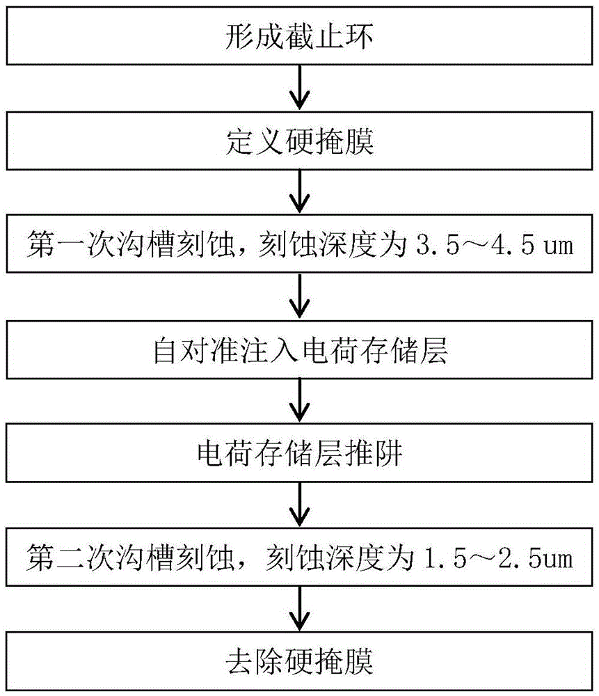
[0050] 1) Provide a lightly doped N-type semiconductor substrate, implant the stop ring, and then push the well to form the stop ring region.
[0051] 2) Form a hard mask, define a gate region by photolithography, etch the gate hard mask, remove glue and clean it, and obtain a defined hard mask.
[0052] Preferably, the material of the hard mask is TEOS, and the deposited thickness is
[0053] Preferably, in other embodiments of the present invention, the material of the hard mask is not limited to TEOS, and other photoresists that can achieve the same effect can be used; the thickness of the hard mask is not limited to The function of the hard mask can be achieved.
[0054] 3) Carry out first trench etching according to the hard mask obtained in step 2), and the etching depth is 3.5-4.5 μm.
[0055] 4) Self-aligned charge storage layer implantation, accurately implanting ions into the s...
Embodiment 2
[0061] A method for forming an IGBT charge storage layer, wherein,
[0062] In step 3), the etching depth is 4 μm, so the depth of the center of the charge storage layer is 4 μm.
[0063] In step 4), the implanted ions are phosphorus, the implanted energy is 40kev, and the implanted amount is 5E12cm -2 ~1E13cm -2 .
[0064] In step 5), the temperature of the well pushing is 115° C., and the well pushing time is 60 min.
[0065] In step 6), the groove is further etched to make the total depth of the groove 6 μm.
[0066] When preparing the charge storage layer through the present invention, the charge storage layer with different charge storage density can be obtained by increasing or decreasing the implant dose; the depth of the charge storage layer can be adjusted by adjusting the etching depth during the first etching position; the time and temperature of pushing the well to the charge storage layer can be adjusted to adjust the diffusion range of the charge storage laye...
Embodiment 3
[0069] A new charge storage type IGBT, including: N-type substrate 21, gate 23, gate oxide layer 23, P well 24, injection region 25, emitter region 26, front metal layer 27, dielectric layer 28, field stop layer 29. Collector region 210 , back metal layer 211 and charge storage layer 212 . Wherein, the charge storage layer 212 is prepared by using the process method provided by the present invention.
[0070] The method for forming the charge storage provided by the present invention can pre-concentrate a large number of ions on the bottom surface layer of the groove etched for the first time, and then adopt relatively mild trapping conditions to form the charge storage layer, and the charge storage layer thus formed It is relatively concentrated, relatively small in thickness, relatively high in ion density, and has a strong charge storage effect, which is obviously different from the charge storage layer formed in the prior art. The charge storage type IGBT provided by the ...
PUM
 Abstract
Description
Claims
Application Information
 - R&D
- Intellectual Property
- Life Sciences
- Materials
- Tech Scout
- Unparalleled Data Quality
- Higher Quality Content
- 60% Fewer Hallucinations
Browse by: Latest US Patents, China's latest patents, Technical Efficacy Thesaurus, Application Domain, Technology Topic, Popular Technical Reports.
© 2025 PatSnap. All rights reserved.Legal|Privacy policy|Modern Slavery Act Transparency Statement|Sitemap|About US| Contact US: help@patsnap.com


