All-solid-state film electrochromic glass and preparation method thereof
An electrochromic glass, all-solid-state technology, applied in chemical instruments and methods, glass/slag layered products, layered products, etc., can solve the problem of unsatisfactory service life and coloring stability, complicated preparation process control, easy ion Diffusion and other problems occur, to achieve the effect of facilitating the production process, reducing production costs and increasing stability
- Summary
- Abstract
- Description
- Claims
- Application Information
AI Technical Summary
Problems solved by technology
Method used
Image
Examples
Embodiment 1
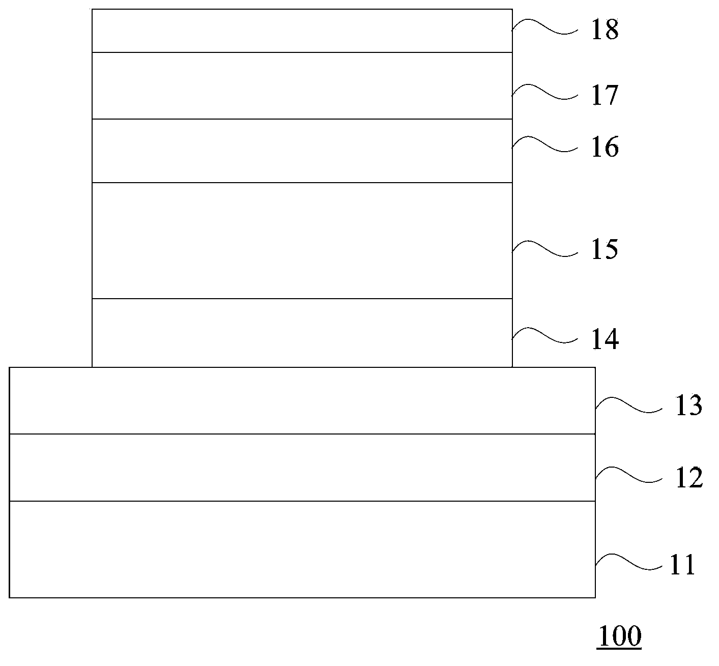
[0028] The film layer structure of the all-solid-state thin-film electrochromic glass is to sequentially form silicon dioxide (SiO 2 ) layer, indium tin oxide (ITO) layer, tungsten oxide (WO 3 ) layer, lithium phosphate nitride (LiPON) layer, lithium cobalt oxide (LiCoO 2 ) layer, indium tin oxide (ITO) layer, silicon nitride (Si 3 N 4 )Floor.
[0029] Its manufacturing process is as follows.
[0030] 6mm ultra-clear glass is washed and dried with pure water and then enters the vacuum coating chamber.
[0031] Intermediate frequency reaction magnetron sputtering silicon oxide target to prepare silicon dioxide layer: set power 30KW, sputtering voltage 450V, pure argon sputtering, gas pressure 3×10 -4 mbar, film thickness 30nm.
[0032] Indium tin oxide layer prepared by magnetron sputtering rotating indium tin oxide target with DC plus pulse power supply: pulse working voltage 800V, DC voltage 180V, pulse frequency 40KHz, set power 60KW, pure argon sputtering, air pressur...
Embodiment 2
[0040] The film structure of the all-solid-state thin-film electrochromic glass is to sequentially form silicon nitride (Si 3 N 4 ) layer, lithium-silver alloy (AgLi) layer, nickel-chromium alloy (NiCr) layer, tungsten oxide (WO 3 ) layer, lithium phosphate nitride (LiPON) layer, lithium cobalt oxide (LiCoO 2 ) layer and low-emissivity (Low-e) composite layer.
[0041] Its manufacturing process is as follows.
[0042] 6mm ultra-clear glass is washed and dried with pure water and then enters the vacuum coating chamber.
[0043] The silicon nitride dielectric layer is deposited by sputtering in an argon-nitrogen atmosphere with an intermediate frequency power supply and a rotating cathode: the vacuum magnetron sputtering equipment is 80-90KW, the frequency of the intermediate frequency power supply is 40KHz, and the thickness is 30nm.
[0044] Magnetron sputtering metallic lithium-silver alloy target to prepare AgLi conductive layer with a thickness of 15nm.
[0045] Prepar...
PUM
| Property | Measurement | Unit |
|---|---|---|
| Thickness | aaaaa | aaaaa |
Abstract
Description
Claims
Application Information
 - R&D
- Intellectual Property
- Life Sciences
- Materials
- Tech Scout
- Unparalleled Data Quality
- Higher Quality Content
- 60% Fewer Hallucinations
Browse by: Latest US Patents, China's latest patents, Technical Efficacy Thesaurus, Application Domain, Technology Topic, Popular Technical Reports.
© 2025 PatSnap. All rights reserved.Legal|Privacy policy|Modern Slavery Act Transparency Statement|Sitemap|About US| Contact US: help@patsnap.com


