Low-temperature radiation electrothermal film and preparation method thereof
A low-temperature radiation and thin-film technology, applied in electric heating devices, ohmic resistance heating, electrical components, etc., can solve problems such as the inability to maintain the uniform dispersion of the ink, the unsatisfactory electrical conductivity of the electrothermal ink, and the reduction of the electrical conductivity of the electrothermal coating. The power can be adjusted flexibly, the electric heating power density is uniform, and the effect of improving the peel strength
- Summary
- Abstract
- Description
- Claims
- Application Information
AI Technical Summary
Problems solved by technology
Method used
Image
Examples
Embodiment 1
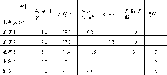
[0071] In the following, the specific use of the ink prepared in the above formula 2 for the preparation of the electric heating film will be described.
[0072] The screen printing templates provided by Shenzhen Bantian Xinstar Screen Printing Materials Co., Ltd. are used. Their specific parameters are as follows. The length and width are 300mm and 200mm respectively, and the screen B is made on both sides of the screen with a length of 7mm. Strip printing side, for printing silver paste, hand-printed with polyurethane squeegee.
[0073] Mesh Wire diameter (micron) Pore size (micron) Thickness (microns) Tension (N / cm) Screen A 325 28 40-50 56 30 Screen B 500 18 30-40 27 25
[0074] The operation steps are as follows:
[0075] (1) Prepare materials and tools: clean screen B and dry it, cut PET film and hot melt adhesive film (M-716A type, thickness about 50 microns) whose length and width are slightly larger than screen B, the th...
Embodiment 2
[0082] Print 3 times in the step of making the carbon nano conductive ink layer, other operations are the same as in Example 1, the thickness of the carbon nano conductive ink is measured to be about 5 microns, and the square resistance measured before the composite upper layer PET film step is 81Ω / □.
Embodiment 3
[0084] The carbon nano conductive ink of formula 3 is used in the step of making the carbon nano conductive ink layer, and other operations are the same as in Example 1. The thickness of the carbon nano conductive ink measured is about 4 microns, and the square resistance measured before the composite upper layer PET film step is 89Ω / □.
PUM
| Property | Measurement | Unit |
|---|---|---|
| Thickness | aaaaa | aaaaa |
| Thickness | aaaaa | aaaaa |
| Thickness | aaaaa | aaaaa |
Abstract
Description
Claims
Application Information
 - R&D
- Intellectual Property
- Life Sciences
- Materials
- Tech Scout
- Unparalleled Data Quality
- Higher Quality Content
- 60% Fewer Hallucinations
Browse by: Latest US Patents, China's latest patents, Technical Efficacy Thesaurus, Application Domain, Technology Topic, Popular Technical Reports.
© 2025 PatSnap. All rights reserved.Legal|Privacy policy|Modern Slavery Act Transparency Statement|Sitemap|About US| Contact US: help@patsnap.com


