
Method of manufacturing build-up printed circuit board

a technology of printed circuit boards and build-up, which is applied in the direction of printed circuit manufacturing, printed circuit aspects, conductive pattern formation, etc., can solve the problems of high product price, difficult realization of fine circuits of core layers, and increased process costs, and achieve high peel strength

Inactive Publication Date: 2007-11-15
SAMSUNG ELECTRO MECHANICS CO LTD
View PDF11 Cites 45 Cited by
  • Summary
  • Abstract
  • Description
  • Claims
  • Application Information

AI Technical Summary

Benefits of technology

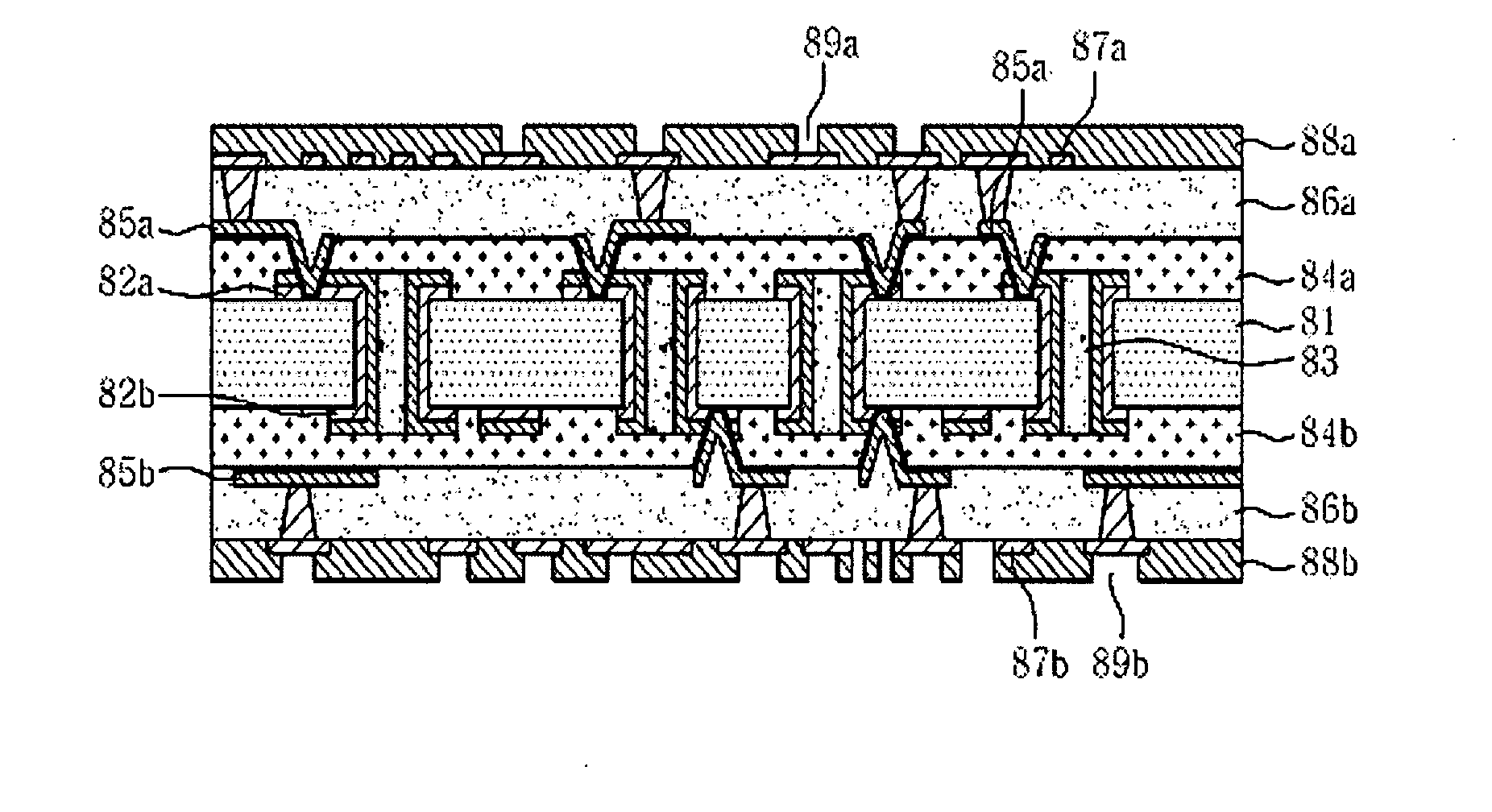
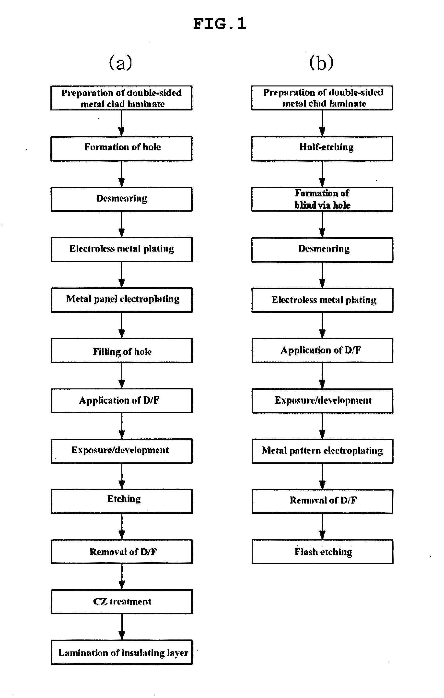
The present invention provides a method of manufacturing a build-up PCB with a core layer and an outer layer using a dry process without using a conventional wet process. The method includes steps of removing metal layers from a resin substrate, surface treatment using ion beams, forming a metal seed layer, and forming a circuit layer through a process called SAP (semi-additive process). The method also includes steps of increasing peel strength between the resin substrate and a metal layer, and realizing a highly reliable fine circuit. The method is environmentally friendly and economical. The technical effects of the invention include achieving a fine circuit through a dry process without using a conventional wet process, and increasing peel strength between the resin substrate and a metal layer.

Problems solved by technology

As such, however, the fine circuit of the core layer is difficult to realize, attributable to the surface roughness of the resin substrate material and the limitation of the subtractive process itself.
However, the use of expensive ABF material results in increased process cost and thus a high product price.
Further, there are limitations in realizing a fine circuit through wet surface treatment and electroless chemical plating.
However, conventional SAP suffers because a metal seed layer is formed through a wet process including wet surface treatment and electroless plating, undesirably increasing the surface roughness, thus making it impossible to realize a fine circuit.
As well, a large amount of waste is generated, causing environmental problems.

Method used


Image

  • Method of manufacturing build-up printed circuit board
  • Method of manufacturing build-up printed circuit board
  • Method of manufacturing build-up printed circuit board

Examples


example 1

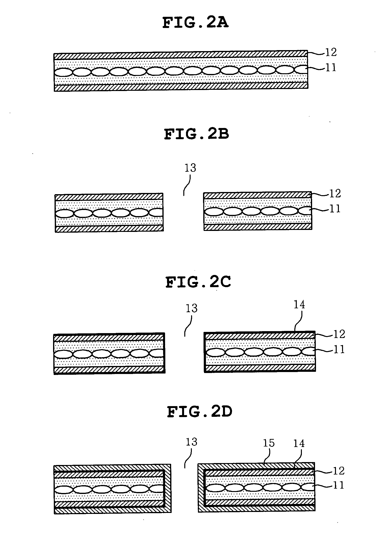
[0073]A. An FR-4 CCL (copper clad laminate) having copper foil laminated on two surfaces thereof was full-etched using an FeCl2 etchant, thus removing the two layers of copper foil. The FR-4 substrate having no copper foil was subjected to mechanical drilling using a CNC (Computer Numerical Control) drill to thus form a via hole having a diameter of about 100˜300 μm, and then to ion beam surface treatment at an acceleration voltage of about 1 KeV and an ion dose of 1E15 using N2 gas. Thereafter, on the surface treated substrate, a Cu seed layer was deposited to a thickness of about 0.3 μm using DC sputtering. Subsequently, a copper pattern plating layer about 10˜20 μm thick was formed through copper pattern electroplating with H2SO4 (120˜160 gl / l), Cu (20˜40 g / l), Cl− (20˜50 ppm), and a cupracid HL leveller (5˜15 ml / l), under conditions of a predetermined air flow volume (0.05˜0.15 m3 / min), temperature (20˜25° C.), and current density (F / B1.5ASD), after which the Cu seed layer was r...

example 2

[0077]An FCBGA was manufactured in the same manner as in Example 1, with the exception that ion beam sputtering was used instead of the DC sputtering, in step A.

[0078]The peel strength of the build-up PCB thus manufactured and the surface roughness of the insulating material were measured. The results are given in Table 1 below.


PUM

PropertyMeasurementUnit
thickaaaaaaaaaa
thickaaaaaaaaaa
diameteraaaaaaaaaa

Abstract

Disclosed is a method of manufacturing a build-up printed circuit board, in which the circuit of a build-up printed circuit board including a core layer and an outer layer is realized by forming the metal seed layer of the core layer using a dry process, consisting of ion beam surface treatment and vacuum deposition, instead of a conventional wet process, including a wet surface roughening process and electroless plating. When the wet process is replaced with the dry process in the method of the invention, the circuit layer can be formed in an environmentally friendly manner, and as well, all circuit layers of the substrate including the core layer and the outer layer can be manufactured through a semi-additive process. Further, the peel strength between the resin substrate and the metal layer can be increased, thus realizing a highly reliable fine circuit.

Description

CROSS REFERENCE TO RELATED APPLICATION[0001]This application claims the benefit of Korean Patent Application No. 10-2006-0042015, filed May 10, 2006, entitled “Process for Build-up Printed Circuit Board”, which is hereby incorporated by reference in its entirety into this application.BACKGROUND OF THE INVENTION[0002]1. Field of the Invention[0003]The present invention relates, in general, to a method of manufacturing a build-up printed circuit board (build-up PCB), and more particularly, to a method of manufacturing a build-up PCB, in which the core circuit layer of a build-up PCB is formed through a dry metal seed layer forming process including ion beam surface treatment and vacuum deposition, thereby realizing a highly reliable fine circuit in an environmentally friendly manner.[0004]2. Description of the Related Art[0005]Presently, build-up PCBs have been manufactured using a subtractive process, a modified semi-additive process (MSAP), and a semi-additive process (SAP).[0006]In...

Claims


Application Information

Patent Timeline
Patent Type & Authority Applications(United States)
IPC IPC(8): H01K3/10H05K3/10H05K3/02
CPCH05K3/108H05K3/146H05K3/381H05K3/4069H05K3/426H05K3/4602Y10T29/49124H05K2203/092H05K2203/1152Y10T29/49165Y10T29/49155Y10T29/49126Y10T29/49128H05K2201/0959H05K1/02H05K3/18
Inventor SONG, JONG SEOKKIM, TAEHOONKIM, DONG SUNCHA, HYE YEON
Owner SAMSUNG ELECTRO MECHANICS CO LTD
Learn More