Ultra-low parasitic ESD protection device

A technology for ESD protection and devices, which is applied in the direction of semiconductor devices, electric solid devices, semiconductor/solid device components, etc., can solve problems affecting impedance matching, affecting circuit impedance matching characteristics, total reflection, etc., and achieve ultra-low parasitic resistance, Excellent discharge capacity and small series resistance

Active Publication Date: 2010-06-02
SEMICONDUCTOR MANUFACTURING INTERNATIONAL (BEIJING) CORP +1
View PDF0 Cites 2 Cited by
  • Summary
  • Abstract
  • Description
  • Claims
  • Application Information

AI Technical Summary

Problems solved by technology

In the weak small signal detection system, the parasitic capacitance 13 will couple the noise from the substrate, and the parasitic resistance 14 will affect the impedance matching. In the high frequency and radio frequency electronic system, if the PAD 12 and the internal circuit input stage are not well Impedance matching may cause partial reflection or even total reflection of the input signal, so that the input signal cannot be sent to the internal system
[0005] Traditional ESD protection devices have their own advantages and disadvantages in their discharge capabilities, but they are all connected to the substrate. The resulting parasitic capacitance will inevitably couple the substrate noise to the internal chip, and the formed parasitic resistance will affect the circuit at high frequencies. Impedance matching characteristics of
Although some people have done research on the traditional ESD device protection model, it is called substrate resistance engineering, but because the parameter extraction of substrate resistance has not been solved so far, it cannot be accurately provided to circuit designers, so I want to use traditional ESD protection devices To protect IC chips (especially high-frequency chips), the effect is not good
If noise and impedance matching problems are serious, even the design's excellent chip performance can be greatly affected

Method used


Image

  • Ultra-low parasitic ESD protection device
  • Ultra-low parasitic ESD protection device
  • Ultra-low parasitic ESD protection device

Examples


Embodiment 1

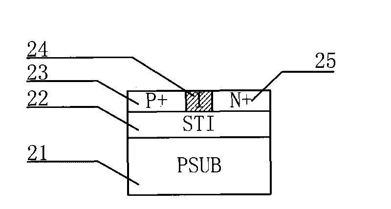
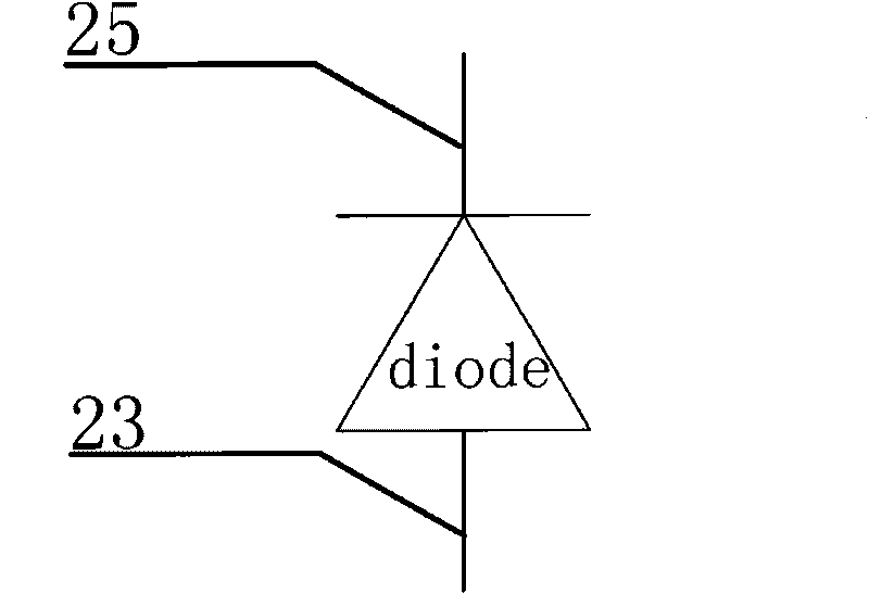
[0031] Such as Figure 4As shown, the ultra-low parasitic ESD protection device provided by the first implementation form of the present invention includes a P+ implantation region 23 and an N+ implantation region 25 arranged on a field oxide layer (not shown in the figure), and an undoped native Constructed region 24, and a plurality of contact holes 26 arranged at intervals on the P+ implanted region 23 and N+ implanted region 25, the contact holes 26 are channels that physically connect the P+ region with the metal or metal compound deposited on the region. The widths of the P+ implantation region 23 and the N+ implantation region 25 are set to the minimum width, and the widths are respectively set to the minimum width of the P+ implantation region and the minimum width of the N+ implantation region of the selected process. Depends on the design rules of the layout, for example, the SMIC0.18um process is 0.43um. The intrinsic region 24 is located between the P+ implantatio...

Embodiment 2

[0033] Such as Figure 5 As shown, the ultra-low parasitic ESD protection device provided by the second implementation form of the present invention includes the P+ implantation region 23 and the N+ implantation region 25 arranged on the field oxide layer (not shown in the figure) as the first embodiment , an undoped intrinsic region 24 and a plurality of contact holes 26 disposed on the P+ implantation region 23 and the N+ implantation region 25 at intervals. The difference between this embodiment and the first embodiment is that the intrinsic region 24 of this embodiment adopts a new type of layout design, and its shape is not linear, but the P+ implantation region 23 and the N+ implantation region 25 are formed in a grid pattern. Alternating implant configurations form arcuate intrinsic regions 24 . The arc-shaped intrinsic region 24 can increase the length of the contact line between the P region and the N region, and increase the junction area of ​​the PN junction. The ...

Embodiment 3

[0036] Such as Figure 6 As shown, it is the ultra-low parasitic ESD protection device provided by the third implementation form of the present invention, which uses multiple single ultra-low parasitic ESD protection devices in Embodiment 2 for parallel connection, and the P-type substrate of this embodiment is connected into one Overall, on the P-type substrate, each single ultra-low parasitic ESD protection device is connected in parallel with each other according to the arcuate contact lines, forming a finger-shaped ESD protection device. This embodiment also includes a P+ implantation region 23 disposed on the field oxide layer (not shown in the figure), an N+ implantation region 25, an undoped intrinsic region 24, a contact hole 26, and a self-aligned metal silicide barrier (Salicideblock) Layer 27, a metal layer (metal) 28 connected to the P+ implantation region and a metal layer (metal) 29 connected to the N+ implantation region. The number of single ultra-low parasiti...


PUM


Abstract

The invention relates to an ultra-low parasitic ESD protection device. The device comprises a P type substrate; a field oxide layer is formed on the P type substrate and is a polysilicon layer; one end of the polysilicon layer is a P+injection region, the other end of the polysilicon layer is a N+injection region, the middle part of the polysilicon layer is an intrinsic region; and a plurality of contact holes are alternately formed on the P+injection region and the N+injection region. Therefore, the ultra-low parasitic ESD protection device has the characteristics of ultra-low parasitic capacitance and ultra-low parasitic resistance, and can ensure excellent releasing capacity.

Description

technical field [0001] The invention relates to a protection circuit of a semiconductor integrated chip, in particular to an ultra-low parasitic ESD protection device which utilizes polysilicon diodes to discharge charges without changing process conditions. Background technique [0002] Electrostatic Discharge (ESD) events of varying degrees will occur in the manufacturing process of the integrated circuit IC chip and in the final system application. Electrostatic discharge is an instantaneous process in which a large amount of charge is poured into the integrated circuit from the outside to the inside when an integrated circuit is floating. The whole process takes about 100ns to 200ns. In addition, when the integrated circuit is discharged, an equivalent high voltage of hundreds or even thousands of volts will be generated, which will break down the gate oxide layer of the input stage in the integrated circuit. As the size of MOS transistors in integrated circuits becomes...

Claims


Application Information

Patent Timeline
Patent Type & Authority Applications(China)
IPC IPC(8): H01L23/60H01L29/868
Inventor 王源俞波贾嵩黄鹏张钢刚张兴
Owner SEMICONDUCTOR MANUFACTURING INTERNATIONAL (BEIJING) CORP
Why Eureka
Try Eureka