
High selectivity Si-rich SiON etch-stop layer

a technology of etchstop layer and si-rich sion, which is applied in the direction of semiconductor/solid-state device manufacturing, basic electric elements, electric devices, etc., can solve the problems of distorted photoresist pattern, increased photolithographic patterning problem, and many of these materials cannot be used

Inactive Publication Date: 2001-06-12
TAIWAN SEMICON MFG CO LTD
View PDF10 Cites 59 Cited by
  • Summary
  • Abstract
  • Description
  • Claims
  • Application Information

AI Technical Summary

Benefits of technology

The use of this dielectric phase antireflective coating (ARC) layer provides several advantages. First, the invention's etch and Si-Rich SiON antireflective coating (ARC) layer allow use of a very thin layer. This decreases the RC delay. The antireflective coating (ARC) layer has superior light absorption qualities beyond other known ARC layers when I line photo processing is used. In addition, the dielectric phase of antireflective coating (ARC) layer is non-conductive and will therefore not produce electrical short circuits of the inlaid damascene structure. In addition, the antireflective coating (ARC) layer may be deposited between the two dielectric layers (or oxide layers) to replace the convention SiN layer so that the antireflective coating (ARC) layer can serve the dual purpose of being an anti-reflective coating and being an etch stop layer used to form the damascene contact. In addition, the antireflective coating (ARC) layer may be deposited directly on top of the underlying conductive region as a barrier layer which prevents atoms of copper or like atoms from diffusing into adjacent dielectric regions.
By using a Si-rich SiON (RI=2.7 measured at a wavelength of 633 nm) ARC layer having a Si molar percentage between about 58% and 62%, better etch selectivity to oxide than that of SiON (RI=2.0 measured at a wavelength of 633 nm) and conventional PE nitride (RI=2.0 measured at a wavelength of 633 nm) is achieved.
.diamond-solid. The thickness of the Si-rich SiON etch-stop layer required for self-aligned dual damascene application can be reduced which decreases the RC delay. The capacitance is inversely proportional to the thickness of the RC delay. Since the invention's Si rich SiON ARC layer and specialized SiO.sub.2 etch process has a high selectivity, the Si rich SiON ARC layer can be thinner thus reducing RC delay.

Problems solved by technology

The semiconductor industry's continuing drive toward integrated circuits with ever decreasing geometries, coupled with its pervasive use of highly reflective materials, such as polysilicon, aluminum, and metal suicides, has lead to increased photolithographic patterning problems.
Unwanted reflections from these underlying reflective materials during the photoresist patterning process often cause the resulting photoresist patterns to be distorted.
A problem with these ARCs is that many of these materials cannot be used in applications such as dual damascene, wherein the metal layer is not patterned.
Some dielectric ARCs are also known, such as conventional silicon rich silicon nitride or aluminum nitride, but a disadvantage with these conventional ARCs is that they are most suitable for deep ultraviolet (DUV) radiation, whereas a vast majority of photolithography steps occur at higher wave lengths such as I-line or G-line where these ARCs are not optimal.
In addition, the dielectric phase of antireflective coating (ARC) layer is non-conductive and will therefore not produce electrical short circuits of the inlaid damascene structure.
However, the selectivity of SiON etch-stop layer to oxide is not high enough when etching the oxide to form interconnect and via hole simultaneously.
There is no selectivity when removing the etch-stop layer after SAC etch, and thus some nitride hardmask and spacer are lost during this step.

Method used


Image

  • High selectivity Si-rich SiON etch-stop layer
  • High selectivity Si-rich SiON etch-stop layer
  • High selectivity Si-rich SiON etch-stop layer

Examples


first embodiment

B. Description of the first embodiment

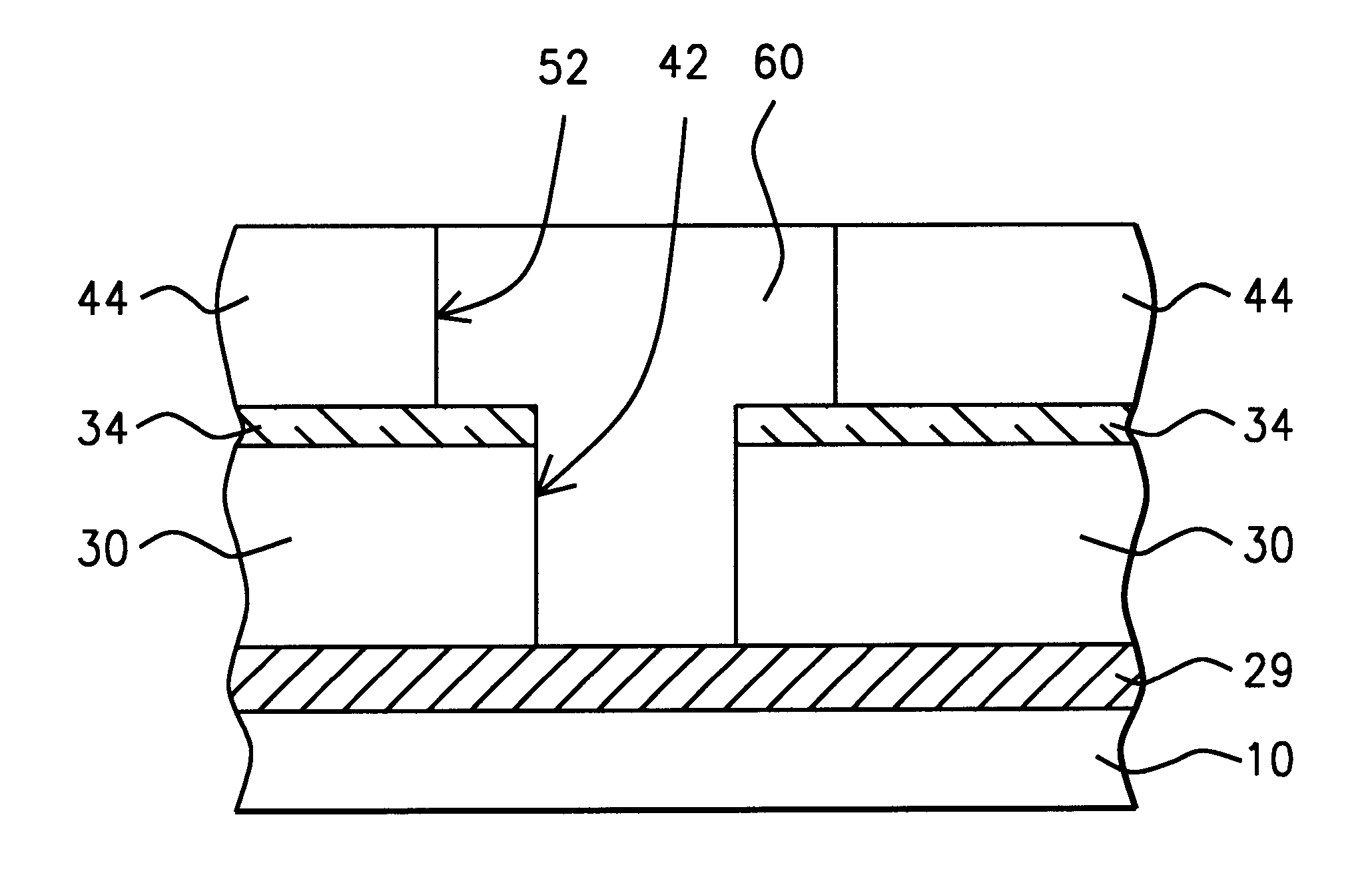
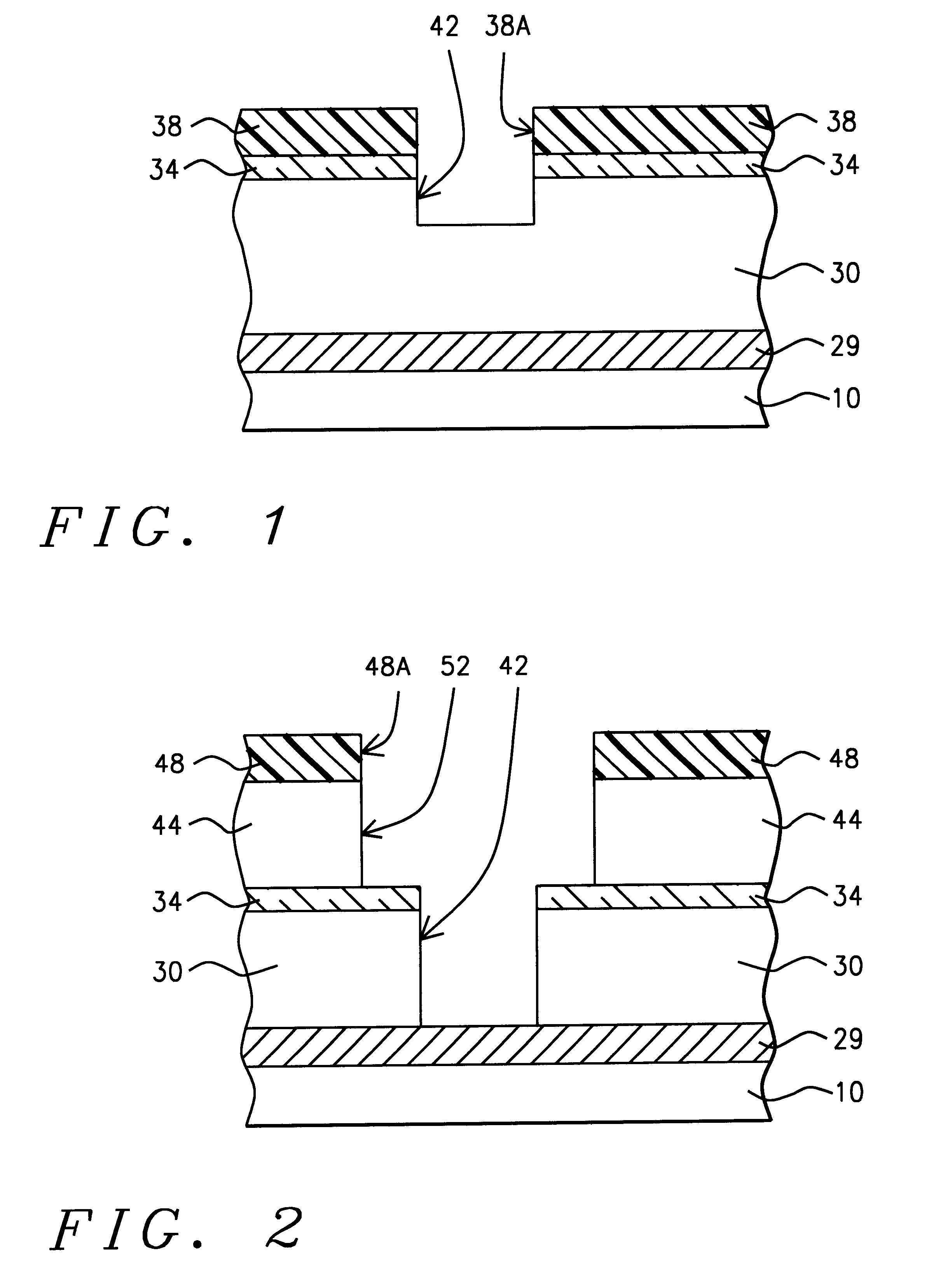
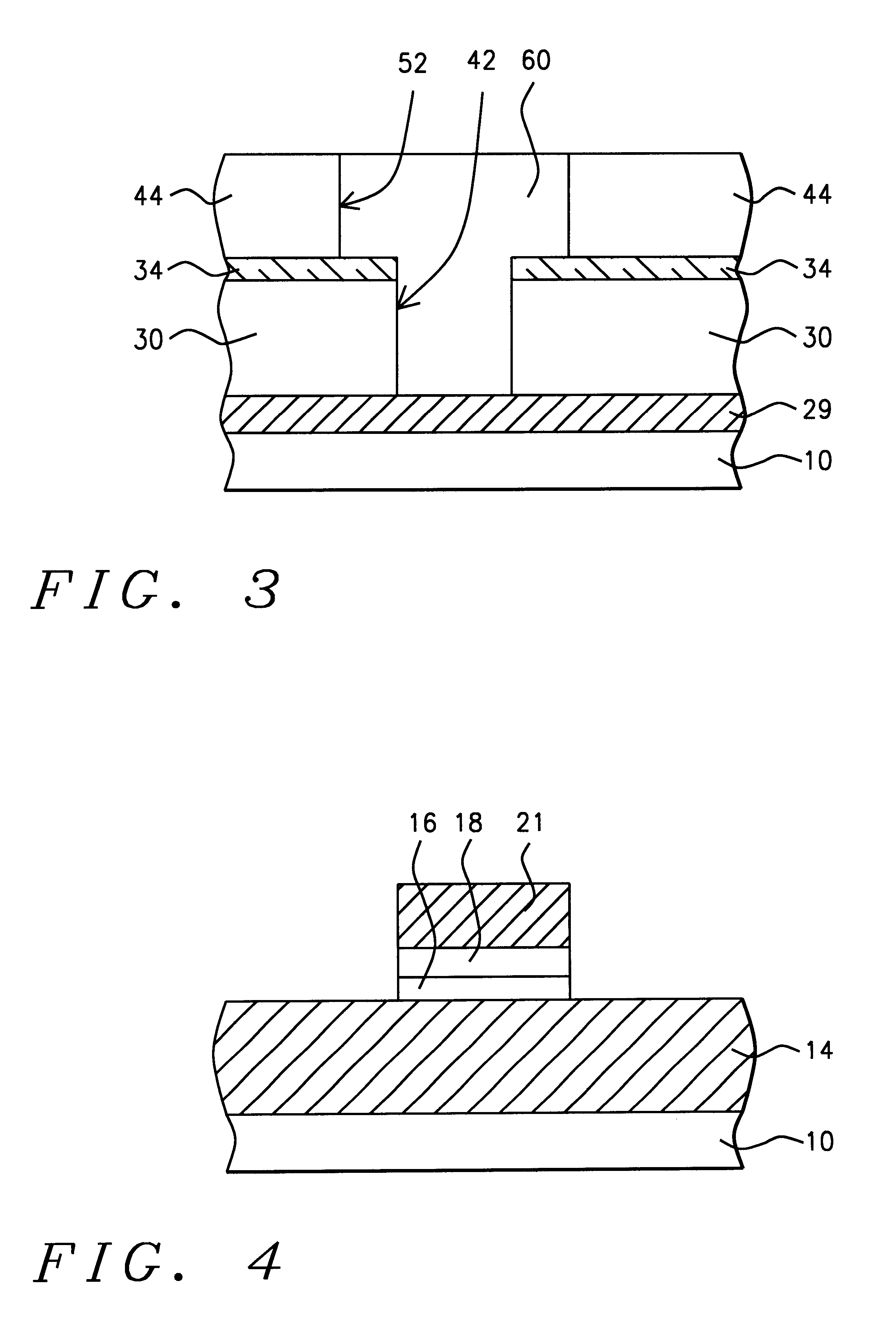
The first embodiment is shown in FIGS. 1 to 3. To begin, a conductive structure 29 of some type is formed over the substrate or semiconductor structure 10. The conductive structure can be a conductive line. The conductive line can preferably be an Al alloy or Cu alloy line. The semiconductor structure can comprise a wafer, with doped regions formed therein and with gates and other devices formed thereon or thereover. An insulating layer can be formed over the wafer and the conductive line can be formed over the insulating layer.

Subsequently, we form a first insulating layer (IMD) 30 over the conductive line 29. The first insulating layer 30 preferably has a thickness of between about 5000 and 10,000 .ANG.. The first insulating layer is preferably composed of Silicon oxide.

C. Invention's Si Rich SiON ARC etch stop layer 34

In a key step, the invention's key Si Rich SiON ARC etch stop layer 34 over the first insulating layer 30. A major advantage o...

second embodiment

SAC With Hard Mask and Spacers Formed of Si Rich SiON

A. Overview of the second embodiment

FIGS. 4 through 8 show a preferred 2.sup.nd embodiment where a self aligned contact (SAC) is formed using special Si Rich Silicon oxynitride spacer layers on the gate electrode 14 and a Si Rich SiON hard mask 18.

The key aspects of the invention for the 2.sup.nd embodiment are:

.diamond-solid. Si rich SiON top hard mask layer 18 and Si rich SiON 2.sup.nd spacer 24

.diamond-solid. oxide etch process to etch oxide layer 30 but is highly selective to the Si rich SiON top hard mask layer 18 and 2.sup.nd spacer 24.

An overview of the major steps of the second embodiment is shown below. The 2.sup.nd embodiment includes the following steps:

a) form a polysilicon layer over a substrate 10;

b) form a hard mask layer on the polysilicon layer; the hard mask layer 1618 comprised of a bottom hard mask 16 on a Silicon oxynitride hard mask 18;

the silicon oxynitride hard mask 18 is preferably composed of Si-rich SiON...


PUM

PropertyMeasurementUnit
RIaaaaaaaaaa
RIaaaaaaaaaa
Pressureaaaaaaaaaa

Abstract

The present invention provides an anti-reflective Si-Rich Silicon oxynitride (SiON) etch barrier layer and two compatible oxide etch processes. The Si-Rich Silicon oxynitride (SiON) etch barrier layer can be used as a hard mask in a dual damascene structure and as a hard mask for over a polysilicon gate. The invention has the following key elements: 1) Si rich Silicon oxynitride (SiON) ARC layer, 2) Special Silicon oxide Etch process that has a high selectivity of Si-Rich SiON to silicon oxide or SiN; 3) Special Si Rich SiON spacer process for a self aligned contact (SAC).A dual damascene structure is formed by depositing a first dielectric layer. A novel anti-reflective Si-Rich Silicon oxynitride (SiON) etch barrier layer is deposited on top of the first dielectric layer. A first opening is etched in the first insulating layer. A second dielectric layer is deposited on the anti-reflective Si-Rich Silicon oxynitride (SiON) etch barrier layer. A second dual damascene opening is etched into the dielectric layers. The anti-reflective Si-Rich Silicon oxynitride (SiON) etch barrier layer can also serve as an ARC layer during these operations to reduce the amount of reflectance from conductive region to reduce distortion of the photoresist pattern.

Description

BACKGROUND OF INVENTION1) Field of the InventionThe present invention relates to semiconductor devices in general, and more particularly to semiconductor devices having anti-reflective coatings and hard masks to aid in photolithography steps, such as those used to form in a dual damascene interconnect structure and gate electrodes.2) Description of the Prior ArtThe semiconductor industry's continuing drive toward integrated circuits with ever decreasing geometries, coupled with its pervasive use of highly reflective materials, such as polysilicon, aluminum, and metal suicides, has lead to increased photolithographic patterning problems. Unwanted reflections from these underlying reflective materials during the photoresist patterning process often cause the resulting photoresist patterns to be distorted.Anti-reflective coatings (ARCs) have been developed to minimize the adverse impact due to reflectance from these reflective materials. In many instances, these ARCs are conductive mat...

Claims


Application Information

Patent Timeline
Patent Type & Authority Patents(United States)
IPC IPC(8): H01L21/02H01L21/70H01L21/027H01L21/033H01L21/768H01L21/314H01L21/311
CPCH01L21/0276H01L21/0332H01L21/0337H01L21/31116H01L21/3144H01L21/3145H01L21/76801H01L21/7681H01L21/76813H01L21/76829H01L21/0214H01L21/02164H01L21/02271H01L21/02211
Inventor FU, CHU YUNTSAI, CHIA SHIUNGJANG, SYUN-MING
Owner TAIWAN SEMICON MFG CO LTD
Learn More