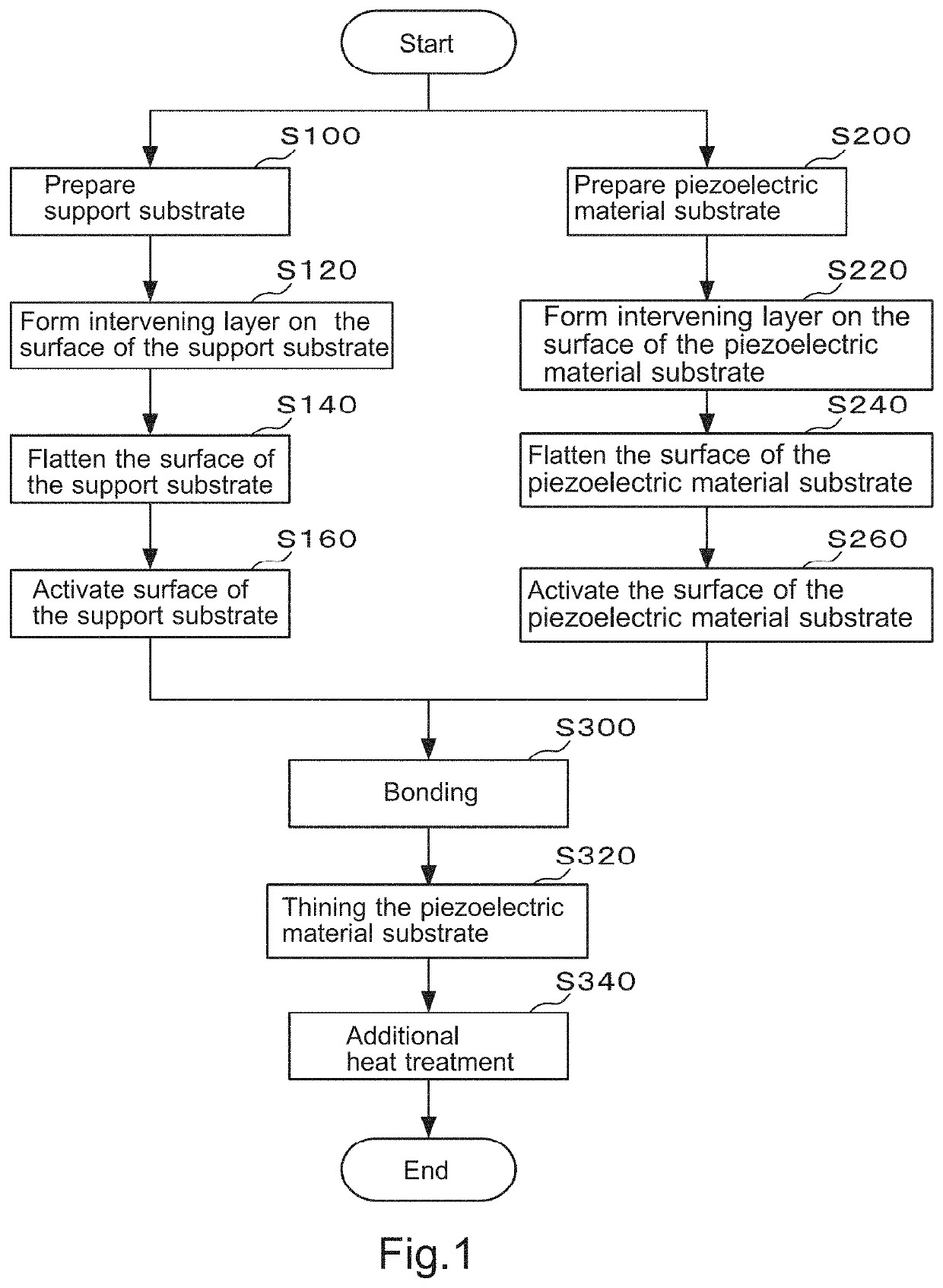
Composite substrate and method of manufacturing composite substrate
a technology of composite substrates and substrates, applied in the field of composite substrates, can solve the problems of low temperature stability, shifted frequency, and difficulty in adjusting the frequency of the corresponding frequency, and achieve the effect of increasing the bonding strength
- Summary
- Abstract
- Description
- Claims
- Application Information
AI Technical Summary
Benefits of technology
Problems solved by technology
Method used
Image


Examples
example 1
[0050]Ten types of 150 mm Φ Si wafers (thickness: 625 μm, P-type, resistivity: around 1100 Ωcm) were prepared, and 150 mm Φ LT wafers (thickness: 250 μm) were bonded together. Table 1 shows the manufacturing method of the single crystal ingot and the oxygen concentration of each of the 10 types of prepared Si wafers. Note that the type of the wafer is represented by a combination of a method for manufacturing a single crystal ingot and a numerical value of an oxygen concentration. For example, 1 ppma wafers produced by the FZ-method were described as “FZ1”.
TABLE 1Wafer typeFZ0FZ1FZ2MCZ2MCZ5MCZ10MCZ12CZ10CZ12CZ15Method ofFZFZFZMCZMCZMCZMCZCZCZCZmanufacturingingotOxygen~012251012101215concentration(ppma)
[0051]It was confirmed that the surface roughness of each of the Si wafer and the LT wafer to be bonded was 0.3 nm or less in Ra (arithmetic mean roughness) The bonding was performed by a room temperature bonding method using a vacuum ion beam. After bonding, the LT wafer was thinned t...
example 2
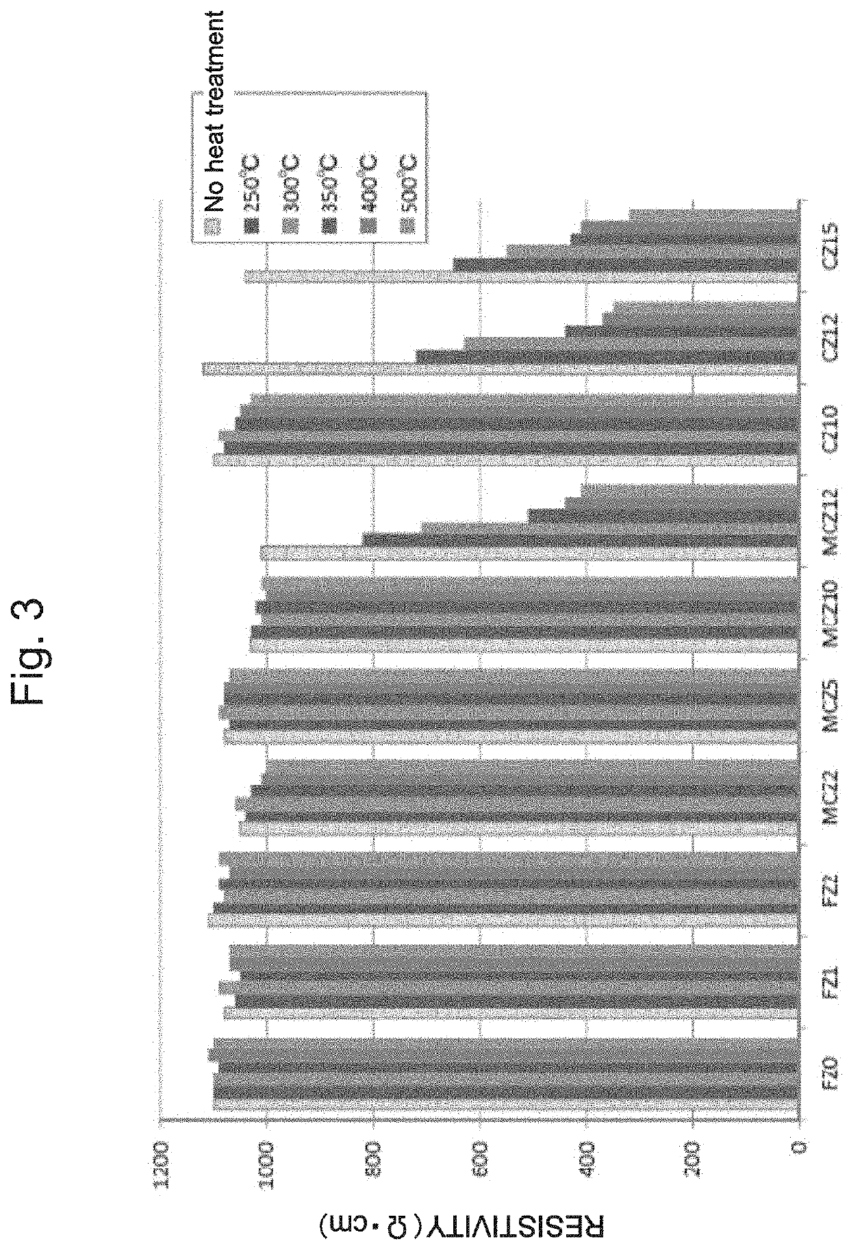
[0052]Ten types of Si wafers were prepared in the same manner as in Example 1, and heat treatment was performed at 250° C., 300° C., 350° C., 400° C., 450° C., and 500° C. for 1 hour in a nitrogen atmosphere. The results of measurement of resistivity before and after heat treatment are shown in Table 3 and FIG. 3. As a result, it was found that, when the oxygen concentration of the Si wafer was 10 ppma or less, there was little change in resistivity even when heat treatment was performed up to 350° C., which is considered to be the maximum temperature of the LT device manufacturing process, regardless of the manufacturing method of the Si single crystal ingot.
TABLE 3Wafer typeFZ0FZ1FZ2MCZ2MCZ5MCZ10MCZ12CZ10CZ12CZ15No heat treatment1100108011101050108010301010110011201040250° C.1100106011001040107010308201080720650300° C.1100109010801060109010107101090630550350° C.1090105010901030108010205101060440430400° C.1110107010701010108010004401050370410500° C.110010701090100010701010410103035...
example 3
[0053]A resonator was produced using the wafers of the 10 kinds of composite substrates obtained in Example 1, and the Q factor was measured. The maximum temperature of the manufacturing process of the resonator, which is an LT device, is about 350° C. For broken wafers, devices are manufactured and measured using surviving portion (i.e., a portion having a size sufficient for manufacturing a device), and for slipped wafers, devices are manufactured and measured using non-slipped portion. The measurement results of the Q factors are shown in Table 4 and FIG. 4. From this result, no deterioration in characteristics was observed for Si wafers having an oxygen concentration of 10 ppma or less, and deterioration in characteristics was observed for Si wafers having an oxygen concentration greater than 10 ppma. This result was found to be consistent with the change in resistivity in Example 2.
TABLE 4Wafer typeFZ0FZ1FZ2MCZ2MCZ5MCZ10MCZ12CZ10CZ12CZ15Q factor250025102500252024802510201024702...
PUM
| Property | Measurement | Unit |
|---|---|---|
| temperature | aaaaa | aaaaa |
| temperature | aaaaa | aaaaa |
| thick | aaaaa | aaaaa |
Abstract
Description
Claims
Application Information
 - R&D
- Intellectual Property
- Life Sciences
- Materials
- Tech Scout
- Unparalleled Data Quality
- Higher Quality Content
- 60% Fewer Hallucinations
Browse by: Latest US Patents, China's latest patents, Technical Efficacy Thesaurus, Application Domain, Technology Topic, Popular Technical Reports.
© 2025 PatSnap. All rights reserved.Legal|Privacy policy|Modern Slavery Act Transparency Statement|Sitemap|About US| Contact US: help@patsnap.com