Gel patterned surfaces
a surface and gel technology, applied in the field of solid phase analytical chemistry, can solve the problems of difficult to predict which if any is amenable to cost-reducing improvements, hindering the technology from moving beyond the research center, and difficult to predict which can be modified
- Summary
- Abstract
- Description
- Claims
- Application Information
AI Technical Summary
Benefits of technology
Problems solved by technology
Method used
Image
Examples
example i
Multiwell Substrates Coated with Silane Free Acrylamide
[0103]This example demonstrates coating of nanowell substrates with silane free acrylamide (SFA), followed by grafting with thiophosphate primers and performing a hybridization of the gel-grafted primers to complimentary fluorescent oligonucleotide to confirm the success of the functionalization approach.
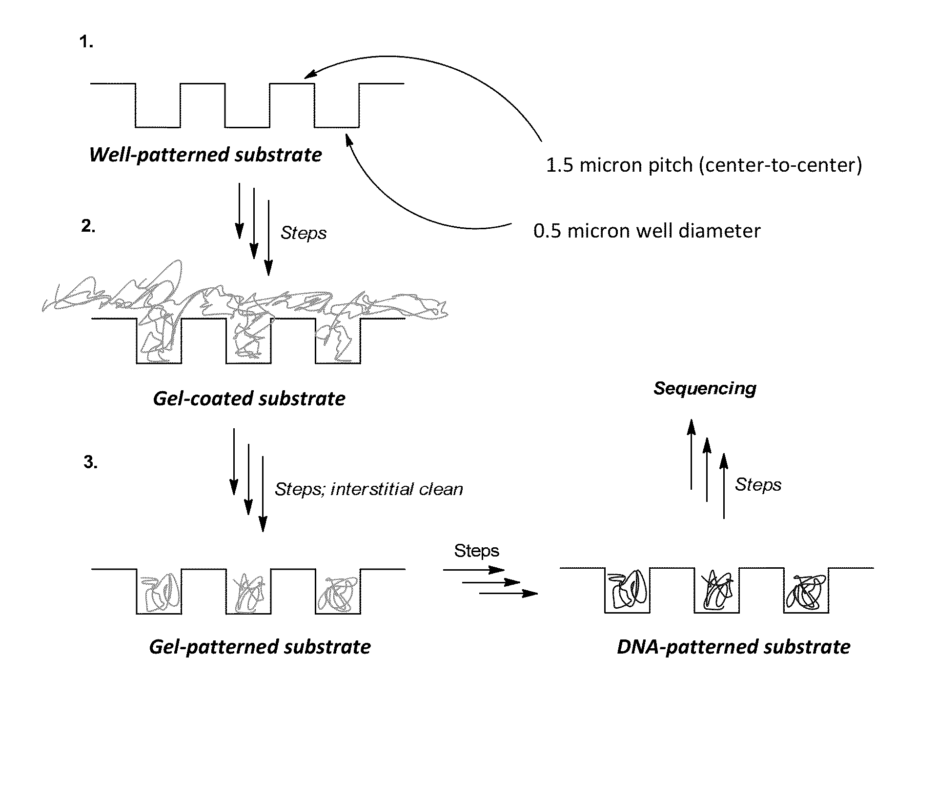
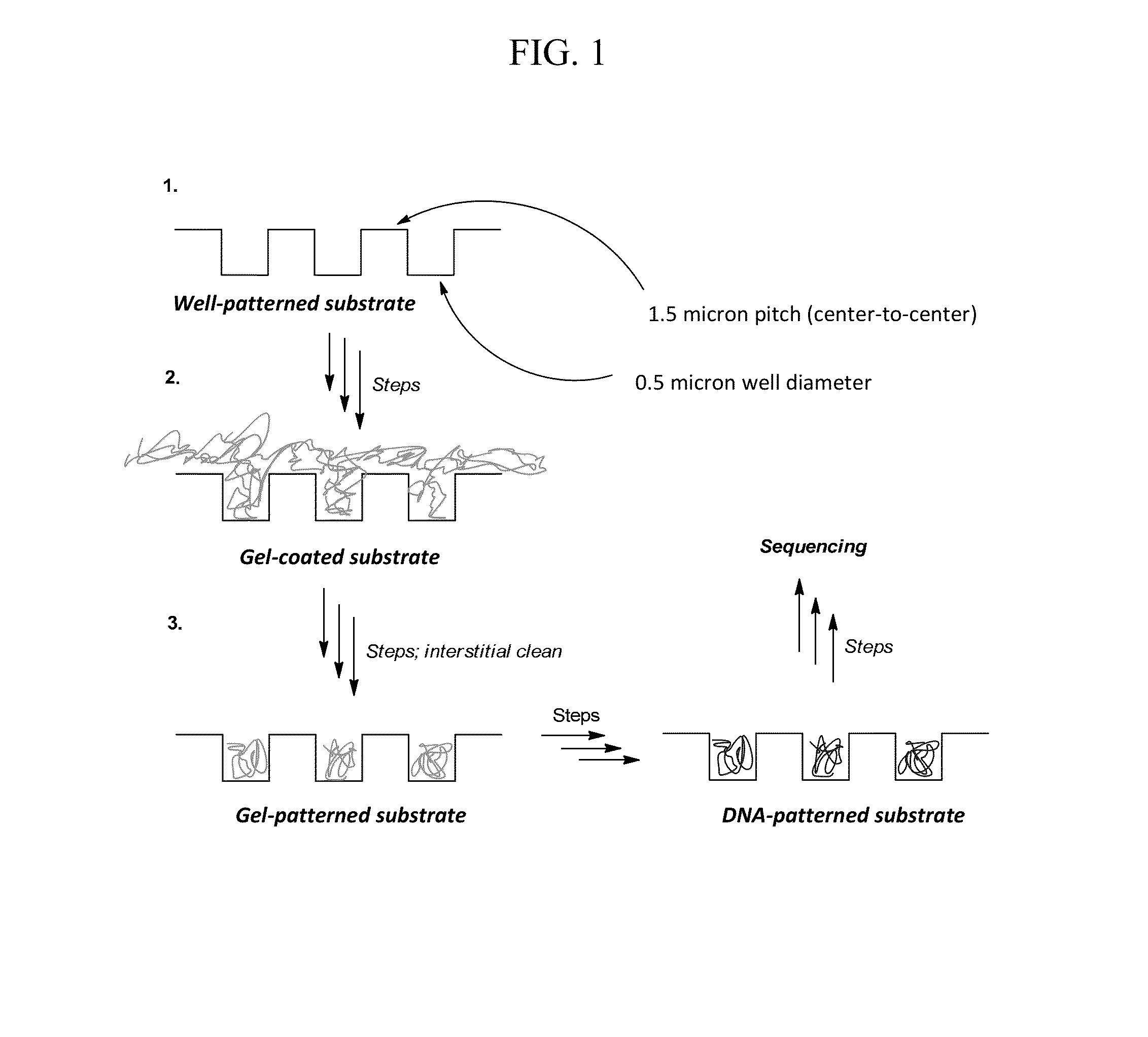
[0104]Chip substrates normally used for manufacture of BeadChips were obtained from Illumina (San Diego, Calif.). The chips were made of silicon or Zeonor (Zeon Corp., Tokyo, Japan) having 0.5 μm wells arranged in a hexagonal pattern having a pitch of 1.5 μm, but the wells did not contain beads beads. The chips were patterned with gel pads as set forth below and diagrammed in FIG. 1.
[0105]The chips were encased in a gasket sealed chamber and oxygen was removed by displacement with fluid reagents for formation of SFA. SFA was polymerized on the chips in the chamber. The reagents for formation of SFA and conditions for polymerizat...
example ii
Fabrication of a Substrate Having Gel-Containing Nanowells
[0108]Multiple techniques can be used to fabricate structured arrays that can subsequently be loaded with gel material.
[0109]The process can start with a blank substrate / wafer and a pattern is introduced into the substrate via micro- or nano-fabrication techniques. The material of the substrate / wafer can be conventional silicon, glass, plastic, COC or any of a variety of materials that can be structured. Exemplary techniques for introducing the patterning into the substrate include photolithography, nanoimprint lithography, embossing of the structures into a plastic / COC based material and injection molding of a plastic or COC into a master mold that has the structures patterned into it. Photolithography based approaches will typically involve use of a photoresist that is patterned with a stepper or mask aligner, exposed with radiation which transfers the pattern present on a reticle / photomask into the photoresist, and then th...
example iii
Multiwell Substrates Coated with PAZAM
[0112]This example shows the fabrication of an array of gel-containing wells, amplification of nucleic acid clusters in the wells and sequencing of the nucleic acids in the clusters.
[0113]Substrates were fabricated as follows. A nanowell substrate (400 nm diameter 1.5 μm pitch, 300 nm depth well) was fabricated using nanoimprint lithography. An amino silane (APTES or APTMS) monolayer / multilayer was deposited on the entire surface of the substrate using chemical vapor deposition. Next, a 1× phosphate buffered saline (pH 7.4) solution of acrylic acid N-hydroxysuccinimide ester (Aldrich PN 8060) at 100 mM concentration was reacted with the amino silane surface by adding 1 ml of the NHS acrylate solution to the surface, covering it with a thin glass coverslip and allowing the reaction to proceed for 1 hour at room temperature. A polymer (PAZAM) was then applied to the surface by spin coating 500 μl of a 2 wt. % PAZAM solution in water onto the newly...
PUM
| Property | Measurement | Unit |
|---|---|---|
| Length | aaaaa | aaaaa |
| Volume | aaaaa | aaaaa |
| Area | aaaaa | aaaaa |
Abstract
Description
Claims
Application Information
 - R&D
- Intellectual Property
- Life Sciences
- Materials
- Tech Scout
- Unparalleled Data Quality
- Higher Quality Content
- 60% Fewer Hallucinations
Browse by: Latest US Patents, China's latest patents, Technical Efficacy Thesaurus, Application Domain, Technology Topic, Popular Technical Reports.
© 2025 PatSnap. All rights reserved.Legal|Privacy policy|Modern Slavery Act Transparency Statement|Sitemap|About US| Contact US: help@patsnap.com


