
Developable bottom antireflective coating compositions especially suitable for ion implant applications

a technology of anti-reflective coating and developer, which is applied in the field of microelectronics, can solve the problems of high reflectivity from the substrate, undetectable high critical dimension (cd) variation of the wafer, and limit the resolution of the resist image, etc., and achieve good reflectivity control, good adhesion to the substrate, and good dissolution properties in the developer

Inactive Publication Date: 2010-08-05
IBM CORP
View PDF10 Cites 23 Cited by
  • Summary
  • Abstract
  • Description
  • Claims
  • Application Information

AI Technical Summary

Benefits of technology

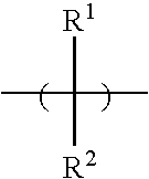
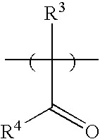
[0008]The invention encompasses developable bottom anti reflective coating (DBARC) compositions comprising a polymer containing pendant aromatic moieties and pendant aliphatic alcohol-containing moieties. These DBARC compositions are characterized by the ability to apply them to substrates using conventional spin-coating and conventional solvents commonly used for casting resist materials. The compositions are further characterized by their ability, upon adequate baking (e.g., above about 150° C.), to undergo little or no significant intermixing with the subsequently applied resist layer. Additionally, the DBARC compositions of the invention provide good reflectivity control (e.g., k value >0.15), good adhesion to substrate, upon adequate baking, and good dissolution properties in developer for the resist. The invention also encompasses methods of using such lithographic structures to pattern underlying material layers on a substrate.

Problems solved by technology

For many lithographic imaging processes, the resolution of the resist image may be limited by anomalous effects associated with refractive index mismatch and undesired reflections of imaging radiation.
High reflectivity from the substrate has become increasingly detrimental to the lithographic performance of photoresists for high NA and short UV wavelength (248 nm and 193 nm) exposures leading to undesirably high critical dimension (CD) variation on the wafer.
This problem is even more pronounced in implant levels owing to the existance of topography (post gate level) and various reflective substrates (such as Si and SiO2 in pregate levels).
Top antireflective coatings (TARC) have been used earlier, but their reflectivity control is not as good as bottom antireflective coatings (BARC).
There is a concern that such etch processes could damage the substrate.
Thus, the use of conventional BARC in the lithography step is not desirable for many applications including implant levels.
Ketones and lactones are usually either not safe enough or not good for spin-coating (the method commonly used to form layers of photoresist materials and BARCs on semiconductor wafers).

Method used


Image

  • Developable bottom antireflective coating compositions especially suitable for ion implant applications
  • Developable bottom antireflective coating compositions especially suitable for ion implant applications
  • Developable bottom antireflective coating compositions especially suitable for ion implant applications

Examples


example 1

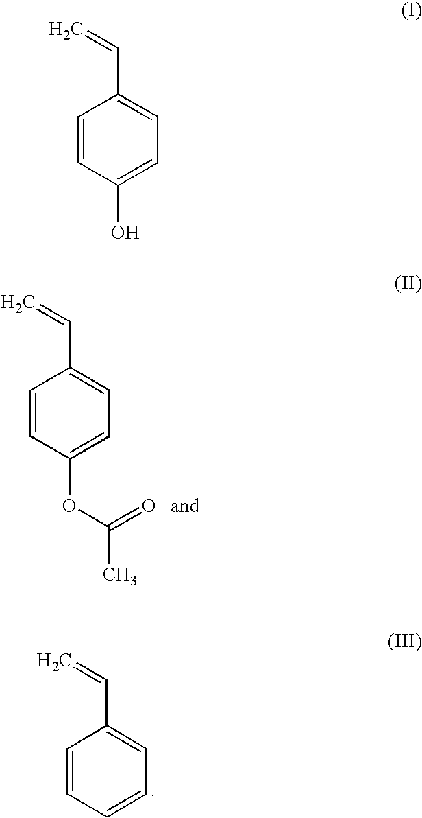
Synthesis of terpolymers of 4-hydroxystyrene, 1-ethylcyclopentyl methacrylate, and 3-hydroxy-1-adamantyl methacrylate (HS / ECpMA / HAdMA(30 / 20 / 50)) (WS-10)

[0060]To a round bottom flask equipped with condenser, thermometer, an argon (Ar) inlet, and a magnetic stirrer bar, the following were added: 4-acetoxystyrene monomer (2.43 grams (g), 0.015 mole), 1-ethylcyclopentyl methacrylate monomer (1.82 g, 0.01 mole), 3-hydroxy-1-adamantyl methacrylate monomer (5.91 g, 0.025 mole), 2,2′-azobis(2-methylpropionitrile) (AIBN)(0.41 g, 5% of total moles of monomers), and approximately 40 g of tetrahydrofuran (THF). The reaction mixture was stirred at room temperature and bubbled with Ar flow for 45 minutes before it was heated. The reaction was carried out overnight at 72° C. under an inert Ar atmosphere. The reaction solution was then cooled to room temperature and approximately 20 g of THF was blown away by a high flow of nitrogen bubbling into the flask. To the remaining reaction solution, 18 g ...

example 2

Synthesis of terpolymers of 4-hydroxystyrene, t-butyl acrylate, and 3-hydroxy-1-adamantyl methacrylate (HS / TBA / HAdMA(30 / 25 / 45)) (WS-17)

[0061]To a round bottom flask equipped with condenser, thermometer, an argon (Ar) inlet, and a magnetic stirrer bar, the following were added: 4-acetoxystyrene monomer (2.43 grams (g), 0.015 mole), t-butyl acrylate monomer (1.6 g, 0.0125 mole), 3-hydroxy-1-adamantyl methacrylate monomer (5.319 g, 0.0225 mole), 2,2′-azobis(2-methylpropionitrile) (AIBN)(0.328 g, 4% of total moles of monomers), and approximately 40 g of tetrahydrofuran (THF). The reaction mixture was stirred at room temperature and bubbled with Ar flow for 45 minutes before it was heated. The reaction was carried out overnight at 72° C. under an inert Ar atmosphere. The rest of the synthetic procedures are the same as Example 1, except approximately 5 g of concentrated NH4OH was used in deprotecting the acetoxy groups from acetoxystyrene repeat units to form hydroxyl styrene repeat unit...

example 3

Patterning of HS / ECpMA / HAdMA(30 / 20 / 50) Polymer

[0062]Formulation was prepared by dissolving 100 mg of polymer prepared in EXAMPLE 1 and 5 mg of TPS PFBuS in 4-methyl-2-pentanol. It was then filtered through 0.2 μm PTFE filter and spincoated onto a clean silicon wafer at about 1500 RPM. The wafer was then baked at 180° C. for 60 sec. Subsequently the wafer was coated with a ArF photoresist and imaged using binary mask in a ArF stepper. The wafer was baked at 100° C. and developed in a standard 0.26N developer. The X-SEM of printed pattern for 135 nm lines / spaces showed improved sidewall profile compared to images created without use of the DBARC of the invention.


PUM


Abstract

Compositions characterized by the presence of an aqueous base-soluble polymer having aromatic moieties and aliphatic alcohol moieties have been found which are especially useful as developable bottom antireflective coatings in 193 nm lithographic processes. The compositions enable improved lithographic processes which are especially useful in the context of subsequent ion implantation or other similar processes where avoidance of aggressive antireflective coating removal techniques is desired.

Description

BACKGROUND OF THE INVENTION[0001]In the microelectronics industry as well as in other industries involving construction of microscopic structures (e.g. micromachines, magnetoresistive heads, etc.), there is a continued desire to reduce the size of structural features. In the microelectronics industry, the desire is to reduce the size of microelectronic devices and / or to provide greater amount of circuitry for a given chip size.[0002]Effective lithographic techniques are essential to achieving reduction of feature sizes. Lithography impacts the manufacture of microscopic structures not only in terms of directly imaging patterns on the desired substrate, but also in terms of making masks typically used in such imaging. Typical lithographic processes involve formation of a patterned resist layer by patternwise exposing the radiation-sensitive resist to an imaging radiation. The image is subsequently developed by contacting the exposed resist layer with a material (typically an aqueous ...

Claims


Application Information

Patent Timeline
IPC IPC(8): G03F7/004G03F7/20
CPCG03F7/0392G03F7/091G03F7/0397
Inventor HUANG, WU-SONGVYKLICKY, LIBORVARANASI, PUSHKARA RAO
Owner IBM CORP
Learn More