Sintered polycrystalline diamond material with extremely fine microstructures
a polycrystalline diamond and microstructure technology, applied in the field of sintered diamond cutting and forming tools, can solve the problems of high cost, anisotropic, limited in size, and inability to provide extremely smooth cut, drawn or otherwise formed workpiece surfaces, and achieve the effects of reducing the cost of pcd tools, and improving the quality of finished products
- Summary
- Abstract
- Description
- Claims
- Application Information
AI Technical Summary
Benefits of technology
Problems solved by technology
Method used
Image
Examples
example 1
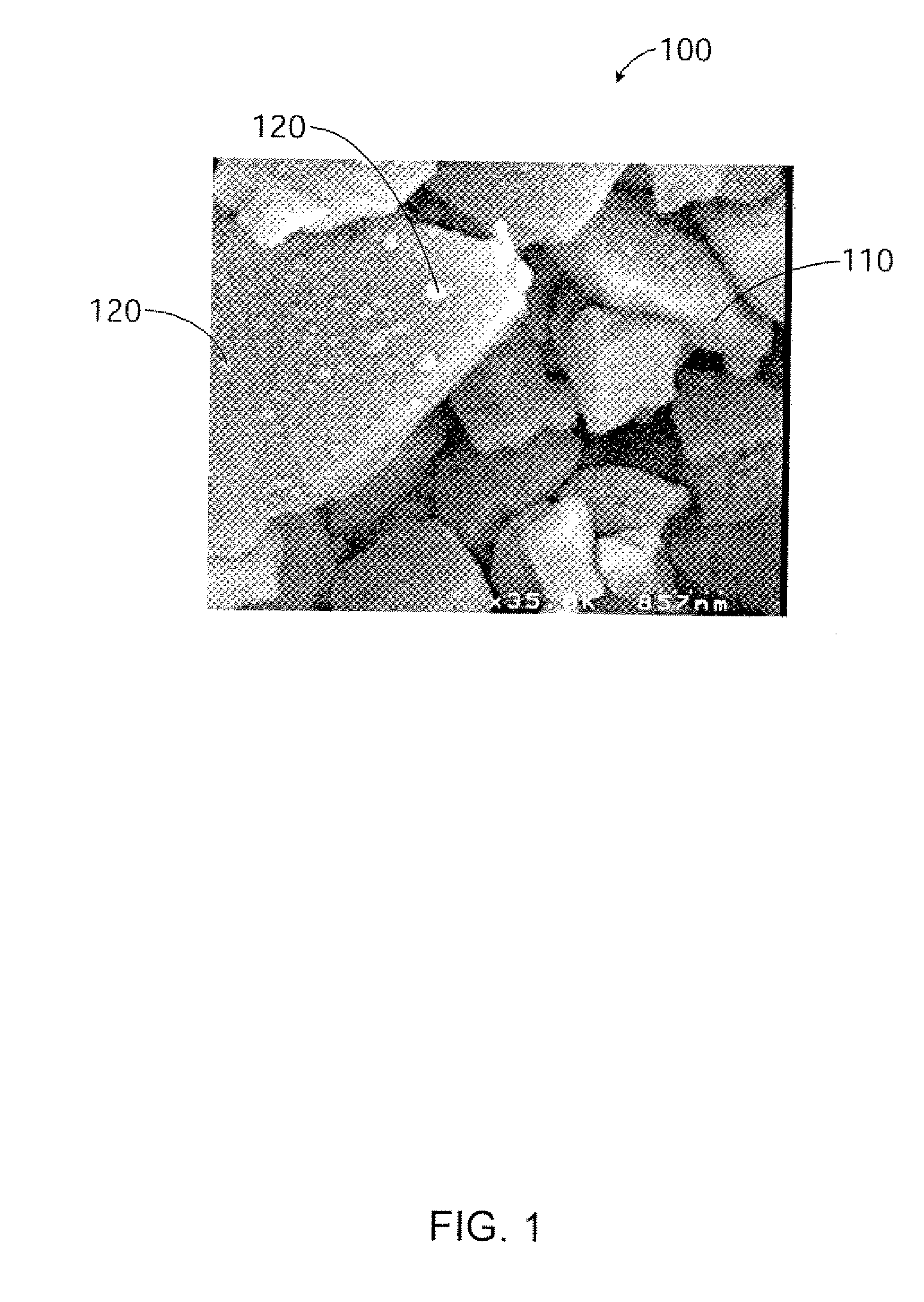
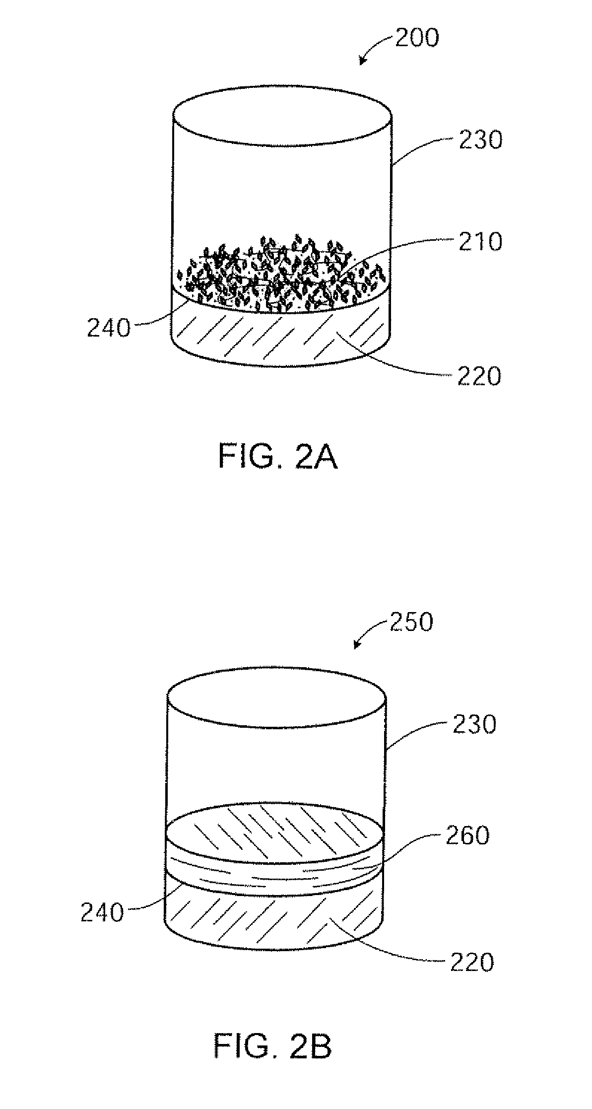
[0042] Referring again to FIGS. 2A and 2B, this example demonstrates the ability to make PCD composites in which the sintered diamond is integrally bonded to a cemented metal carbide substrate. A diamond-cobalt powder blend with approximately 7% cobalt by weight, distributed as shown in FIG. 1 with approximately 0.8 μm volumetric mean raw material diamond size 210, was disposed between a tantalum (Ta) shielding enclosure 230 and a cemented tungsten carbide (WC)+13 weight-percent cobalt disk. This assembly was subjected to HP / HT processing at about 55 Kbar at temperature of about 1400° C. for about 20 minutes to form the sintered submicron PCD tool blank 260. The PCD tool blank 250 was finished to produce a diamond layer 260 1.5 mm thick, and the overall thickness of the blank 250 was 3.2 mm. The average as-sintered diamond grain size, assessed by direct line intercept measurement of the microstructure with a field emission scanning electron microscope, was 0.87 μm. Several variation...
example 2
[0048] Referring to FIG. 8, this example illustrates the ability to make carbide supported wire die blanks 800. These are materials in which the diamond portion 810 is sintered into a carbide annulus 820 using a separate metal source as the catalyst rather than sintering using the cobalt binder phase from the carbide substrate. In this example, diamond powder 810 with a volumetric mean particle size of 0.5 μm further containing 7% by weight of the fine, dispersed cobalt similar to Example 1 was used. The diamond and cobalt powder blend 810 were loaded into the center of a carbide cylinder 820 encased in a tantalum (Ta) enclosure 830. A cobalt (Co) disc 840 (shown in exploded view) was placed on top of the powder followed by a Ta shielding enclosure 850 (also in exploded view), Several of these assemblies were loaded into a HP / HT reaction cell and subjected to pressures of about 55 Kbar at temperatures between about 1300° C. and about 1500° C. for about 15 minutes to form the sintere...
PUM
| Property | Measurement | Unit |
|---|---|---|
| grain size | aaaaa | aaaaa |
| grain size | aaaaa | aaaaa |
| grain size | aaaaa | aaaaa |
Abstract
Description
Claims
Application Information
 - R&D
- Intellectual Property
- Life Sciences
- Materials
- Tech Scout
- Unparalleled Data Quality
- Higher Quality Content
- 60% Fewer Hallucinations
Browse by: Latest US Patents, China's latest patents, Technical Efficacy Thesaurus, Application Domain, Technology Topic, Popular Technical Reports.
© 2025 PatSnap. All rights reserved.Legal|Privacy policy|Modern Slavery Act Transparency Statement|Sitemap|About US| Contact US: help@patsnap.com


