Method to recover the exposure sensitivity of chemically amplified resins from post coat delay effect

a technology of delay effect and exposure sensitivity, which is applied in the field of semiconductor processing methods, can solve the problems of increasing data volume, changing stability and radiation dose sensitivity, and increasing the requirement for critical dimension control and throughput on photomask manufacture, etc., and achieves the effect of reducing the shelf life of ca resists or prolonging the shelf life of ca resists

Inactive Publication Date: 2005-08-04
MICRON TECH INC
View PDF11 Cites 1 Cited by
  • Summary
  • Abstract
  • Description
  • Claims
  • Application Information

AI Technical Summary

Benefits of technology

[0019] The present invention solves the problem of maintaining a uniform and reproducible pattern critical dimension in a CA resist from the time of application of the resist onto a substrate to and during a writing process for imaging a photomask. The process of the invention eliminates, or substantially reduces, the sensitivity of a CA photoresist to the environment and maintains the pattern critical dimension of the resist to extend the shelf life of the CA resist during storage in handling which may be for a time period up to weeks, and during direct write imaging of the photoresist by either optical or e-beam radiation. The process of the invention significantly improves the lithographic performance in terms of critical dimension and integrity of the photoresist. The invention advantageously eliminates unnecessary work to calibrate the post coat delay (PCD) effect, and increases the accuracy and reproducibility of CD performance.

Problems solved by technology

With the fast pace of reduction of the micro-lithography design rule and the significant increase of data volume, the requirement on critical dimension (“CD”) control and throughput on a photomask manufacture is becoming more and more challenging.
However, in practice, resist-coated blanks are often stored for several hours up to weeks before exposure.
A difficulty with the use of CA resists is the change in stability and radiation dose sensitivity that occurs when a CA resist is coated on a substrate that is left standing inside or outside an irradiation apparatus.
Development of CA resists depends on the catalytic action of the acid generator, and if acid loss (neutralization) occurs, which decreases the radiation dose sensitivity of the resist, abnormalities will occur during pattern formation resulting in a significant difference between critical dimensions (CD) (i.e., minimum feature dimensions) of the patterned features compared to the required pattern dimensions.
The acid loss is believed to be due to the presence of nitrogen-containing compounds such as atmospheric ammonia or ammonium ions, which neutralize the acid generator resulting in incomplete solubility of the resist, thus limiting shelf life of a photomask blank with an applied CA resist layer.
While use of these known methods produces some improvement over an untreated substrate, significant profile defects are still evident.

Method used


Image

  • Method to recover the exposure sensitivity of chemically amplified resins from post coat delay effect
  • Method to recover the exposure sensitivity of chemically amplified resins from post coat delay effect
  • Method to recover the exposure sensitivity of chemically amplified resins from post coat delay effect

Examples


Embodiment Construction

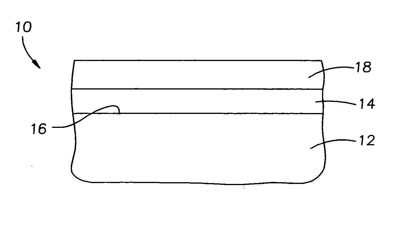
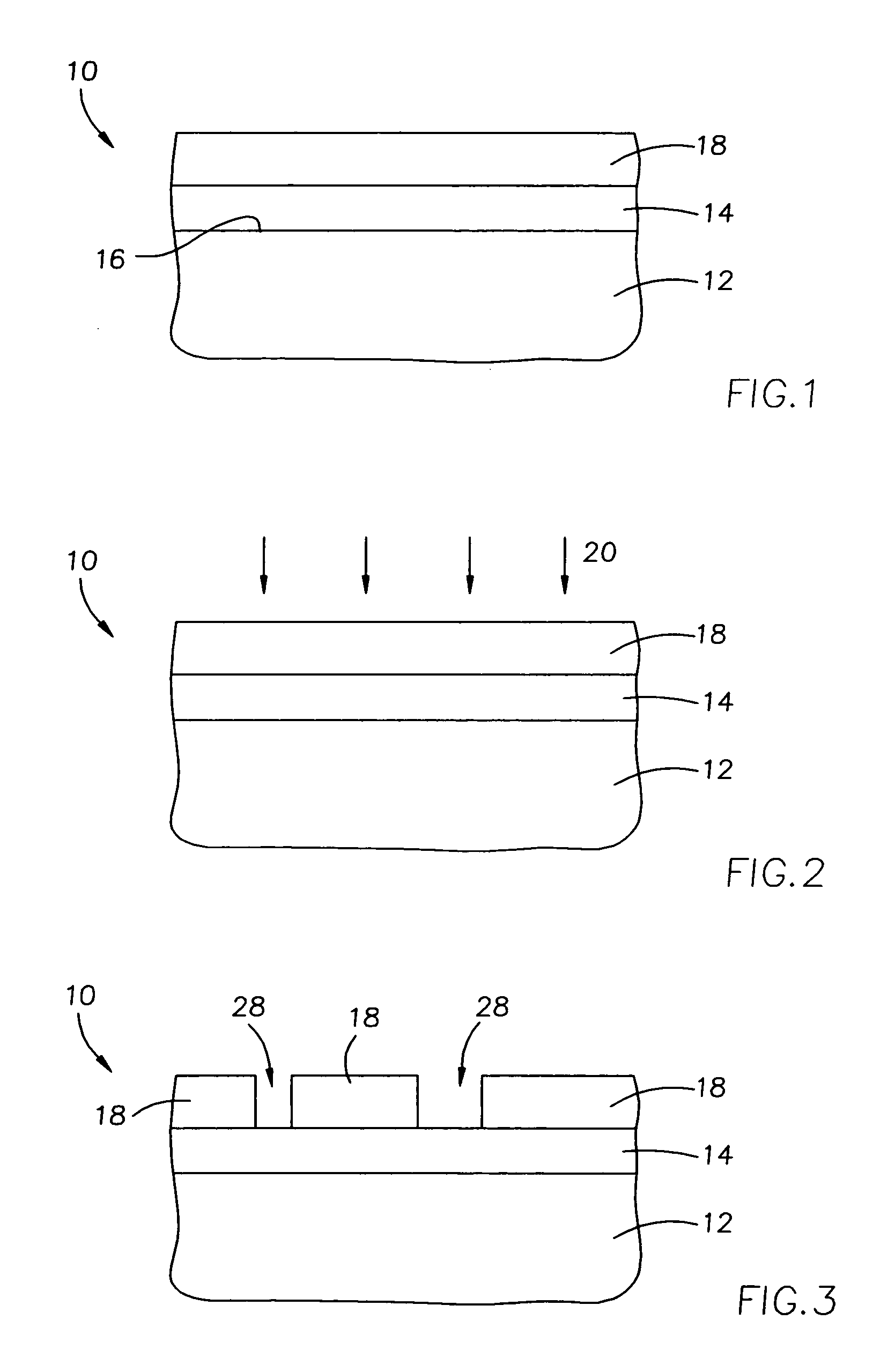
[0025] The invention will be described generally with reference to the drawings for the purpose of illustrating the present preferred embodiments only and not for purposes of limiting the same. The figures illustrate processing steps for fabricating photomask in accordance with the present invention. It should be readily apparent that the processing steps are only a portion of the entire fabrication process.

[0026] In the current application, the terms “semiconductive substrate”, “semiconductor substrate”, “wafer fragment” or “wafer” will be understood to mean any construction comprising semiconductive material, including but not limited to bulk semiconductive materials such as a semiconductor wafer (either alone or in assemblies comprising other materials thereon), and semiconductive material layers (either alone or in assemblies comprising other materials). The term “substrate” refers to any supporting structure, including, but not limited to, the semiconductive substrates describ...


PUM

PropertyMeasurementUnit
temperatureaaaaaaaaaa

Abstract

Methods of fabricating a photomask, methods of treating a chemically amplified resist-coated photomask blank, a photomask blank resulting from the methods, and systems for fabricating a photomask are provided. The method is useful for recovering the exposure sensitivity of a chemically amplified resist disposed on a photomask blank from a post-coat delay effect.

Description

CROSS REFERENCE TO RELATED APPLICATION [0001] This application is a divisional of U.S. patent application Ser. No. 10 / 391,708, filed Mar. 19, 2003.FIELD OF THE INVENTION [0002] The invention relates generally to semiconductor processing methods, and more particularly to processes for fabricating a photomask that can be used in a photolithography process. BACKGROUND OF THE INVENTION [0003] Photolithography using a patterned masking layer is commonly used for formation of electronic components such as semiconductor integrated circuits. A pattern is transferred to a reactive photoresist layer on the semiconductor substrate by exposure of the patterned masking layer overlying the substrate to light or other energy source (such as ultraviolet light or electron beam radiation) which passes through open areas of the patterned masking layer. [0004] The masking layer can be, for example a photomask or reticle, prepared from a photomask blank that typically comprises a thin layer of an opaque...

Claims


Application Information

Patent Timeline
Patent Type & Authority Applications(United States)
IPC IPC(8): G03F1/00G03F7/039G03F7/16
CPCG03F1/14G03F7/168G03F7/039G03F1/50
Inventor YANG, BAORUI
Owner MICRON TECH INC
Why Eureka
Try Eureka