Temporary self-aligned stop layer is applied on silicon sidewall

a technology of silicon sidewall and stop layer, applied in the direction of semiconductor devices, electrical apparatus, transistors, etc., can solve the problems of increasing the resistivity of source/drain regions, affecting device performance, and difficult to achieve both desirable features at the same time, so as to reduce the series resistance of shallow areas

Inactive Publication Date: 2005-07-14
TAIWAN SEMICON MFG CO LTD
View PDF10 Cites 22 Cited by
  • Summary
  • Abstract
  • Description
  • Claims
  • Application Information

AI Technical Summary

Benefits of technology

[0014] One objective of the present invention is to provide a means of forming a MOSFET or MOS transistor having silicide contacts to the gate electrode and source / drain regions that are electrically isolated, said contacts will reduce the series resistance of the shallow and deep source / drain regions.
[0016] A still further objective of the present invention is to provide a method of fabricating a MOS transistor that prevents shorting or bridging between the silicide on the gate electrode and the silicide over the source / drain regions.
[0017] A still further objective of the present invention is to provide a reliable and manufacturable method of forming a MOSFET with shallow source / drain regions and a salicide structure used in fabricating an integrated circuit device.
[0019] Next, a first photoresist layer is coated and patterned to protect the second active region over the P-well and uncover the first active region over the N-well. A first implant is performed in which a p-type dopant such as BF2+ ions are implanted into the first active region including the first gate electrode and adjacent sidewall spacers and silicon sidewalls. The first photoresist layer is removed and then a second photoresist layer is coated and patterned to protect the first active region and uncover the second active region. A second implant is performed in which an n-type dopant such as P31+ ions are implanted into the second active region including the second gate electrode and adjacent sidewall spacers and silicon sidewalls. After the second photoresist is removed, a rapid thermal anneal (RTA) of the substrate activates the source / drain regions as the impurity ions from both implants are driven into the substrate in active regions underlying the thin oxide etch stop layer to form deep source / drain regions. Meanwhile, a thermal solid phase diffusion of the impurity ions from the silicon sidewalls into the substrate forms shallow source / drain regions adjacent to the deep source / drain regions. The thin silicon oxide etch stop layer prevents out diffusion of the dopant from the deep source / drain regions.
[0020] Next, the thin etch stop layer is removed. A metal layer that is preferably titanium is deposited and an RTA is used to form a silicide layer where the metal is in contact with silicon. In other words, a silicide layer is formed above the gate electrode and above the deep / source drain regions and on the silicon sidewalls. Unreacted metal is removed in a subsequent step which results in an extended silicide layer that reduces the series resistance of the source / drain regions and prevents short channel effects

Problems solved by technology

A second problem with short channels is an increase in the resistivity of source / drain regions because of a shallower depth and a smaller conductive area.
For conventional LDD structures, there is a trade-off between an ultra-shallow junction region and a high impurity concentration and it is difficult to achieve both desirable features at the same time.
However, the depth and uniformity of ion implants in shallow source / drain regions may be difficult to control and may lead to a degradation in device performance.
One drawback is that the dopant must pass through a silicon oxide layer before it reaches the substrate and this extra layer diminishes the concentration of impurity ions in the LDD region.
However, during the oxide formation, some of the implanted ions may diffuse out of the substrate and reduce the dopant concentration.
This process is more complicated because of the additional ion implant step and the laser radiation which must be carefully controlled to avoid melting adjacent substrate regions.

Method used


Image

  • Temporary self-aligned stop layer is applied on silicon sidewall
  • Temporary self-aligned stop layer is applied on silicon sidewall
  • Temporary self-aligned stop layer is applied on silicon sidewall

Examples


second embodiment

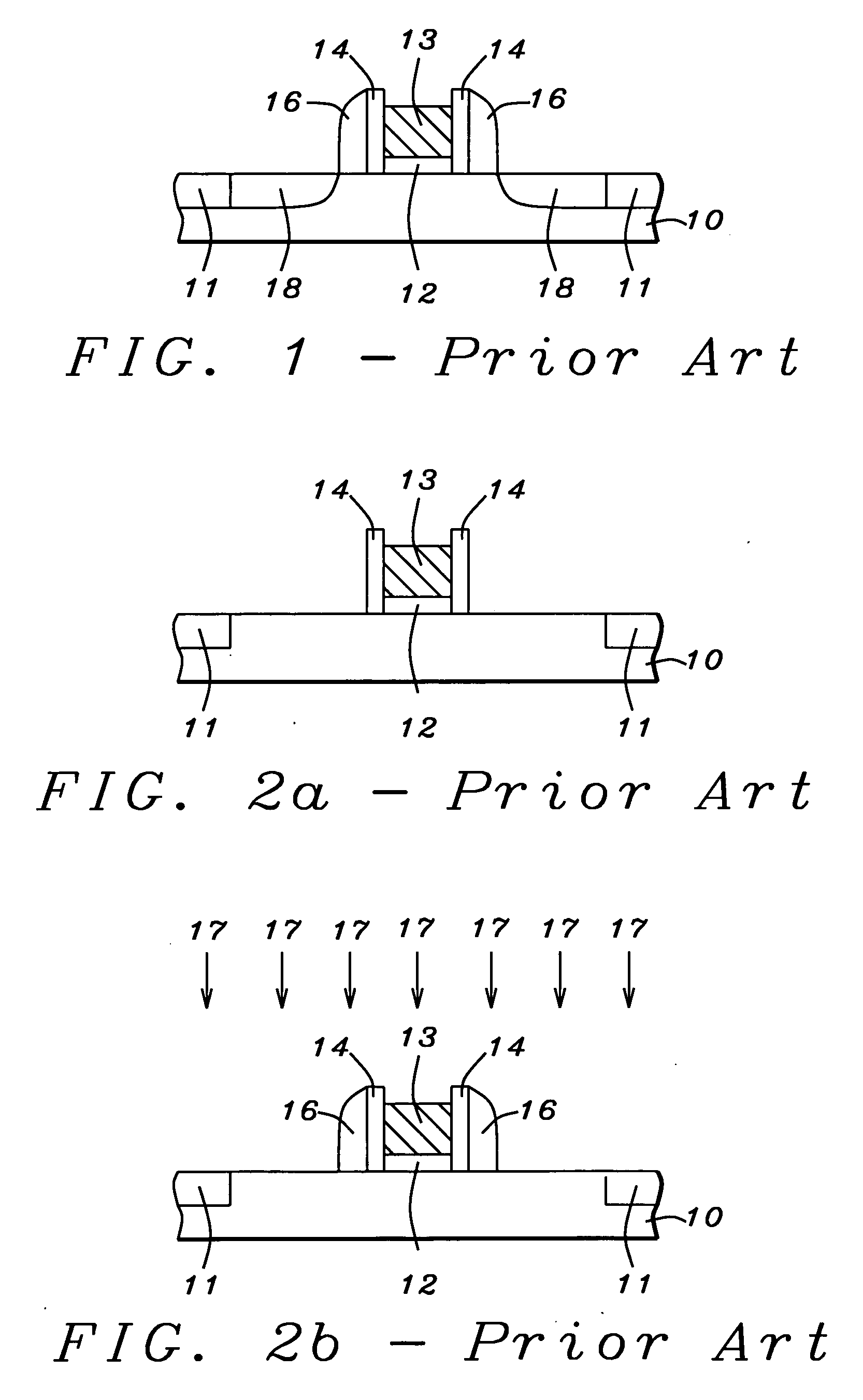
[0026] The present invention is a method of forming a transistor on a semiconductor substrate in which silicon sidewalls are formed adjacent to first sidewall spacers next to a gate electrode. The silicon sidewalls enable an extended salicide structure to be fabricated in a subsequent sequence of steps that lead to a lower resistivity. In one embodiment, a method is provided for forming NMOS and PMOS transistors simultaneously on a substrate. In a second embodiment, a method is described for fabricating a MOS transistor according to the present invention. The drawings are provided by way of example and are not intended to limit the scope of the invention

first embodiment

[0027] The first embodiment is illustrated in FIGS. 3a-3h. Referring to FIG. 3a, a substrate 20 is provided with isolation regions 21 that may be shallow trench isolation (STI) regions, for example. The isolation regions 21 separate a first active region 22a that includes an N-well 26 from a second active region 22b that has a P-well 27. The substrate 20 is preferably monocrystalline silicon. The isolation regions 21 are typically comprised of silicon oxide or a low k dielectric material such as carbon doped SiO2 or fluorine doped SiO2. Field oxide (FOX) regions or mesa isolation regions known to those skilled in the art may be used instead of STI regions.

[0028] A gate dielectric layer 23 is formed on the substrate 20 by a conventional method and may be comprised of silicon oxide or a high k dielectric material such as Ta2O5, TiO2, Al2O3, ZrO2, HfO2, Y2O3, La2O5 and their aluminates and silicates. A gate that is preferably comprised of polysilicon having a thickness between about 15...


PUM

PropertyMeasurementUnit
widthaaaaaaaaaa
widthaaaaaaaaaa
thicknessaaaaaaaaaa

Abstract

A method is provided for forming NMOS and PMOS transistors with ultra shallow source / drain regions having high dopant concentrations. First sidewall spacers and nitride spacers are sequentially formed on the sides of a gate electrode followed by forming a self-aligned oxide etch stop layer. The nitride spacer is removed and an amorphous silicon layer is deposited. The etch stop layer enables a controlled etch of the amorphous silicon layer to form silicon sidewalls on the first sidewall spacers. Implant steps are followed by an RTA to activate shallow and deep S / D regions. The etch stop layer maintains a high dopant concentration in deep S / D regions. After the etch stop is removed and a titanium layer is deposited on the substrate, an RTA forms a titanium silicide layer on the gate electrode and an extended silicide layer over the silicon sidewalls and substrate which results in a low resistivity.

Description

RELATED PATENT APPLICATION [0001] This application is related to the following: Docket # TS00-350, Ser. No. 10 / 279,898, filing date Oct. 24, 2002, assigned to a common assignee.FIELD OF THE INVENTION [0002] The invention relates to a method of fabricating an integrated circuit in a semiconductor device. More particularly, the present invention is directed to a method of manufacturing NMOS and PMOS transistors with shallow junctions and an extended salicide structure. BACKGROUND OF THE INVENTION [0003] As technology advances into the regime of sub-100 nm gate lengths in order to increase transistor speed in MOSFET (Metal Oxide Semiconductor Field Effect Transistor) devices, there is a need to improve the performance of source / drain regions which define the channel length. A conventional MOSFET as fabricated in prior art is shown in FIG. 1 and is comprised of a substrate 10 with insulating regions 11 such as shallow trench isolation (STI) regions that separate active areas upon which ...

Claims


Application Information

Patent Timeline
Patent Type & Authority Applications(United States)
IPC IPC(8): H01L21/3213H01L21/336H01L21/8238
CPCH01L21/32137H01L21/823814H01L21/823835Y10S257/90H01L29/6653H01L29/6656H01L29/6659H01L29/665
Inventor CHO, SHU-YINGCHUNG, CHIEN-MINGHUANG, YUAN-CHANG
Owner TAIWAN SEMICON MFG CO LTD
Why Eureka
Try Eureka