
Epitaxial wafer, epitaxial wafer growth method and high electron mobility transistor

A growth method and epitaxial wafer technology, applied in the directions of crystal growth, single crystal growth, single crystal growth, etc., can solve the problems of leakage, reduce device performance, cannot achieve high resistance, etc., to improve crystal quality, reduce leakage, and improve clamping. The effect of breaking characteristics and withstand voltage characteristics

Pending Publication Date: 2022-05-27
JIANGXI ZHAO CHI SEMICON CO LTD
View PDF0 Cites 1 Cited by
  • Summary
  • Abstract
  • Description
  • Claims
  • Application Information

AI Technical Summary

Problems solved by technology

However, since the oxygen atoms decomposed from the oxide (such as SiO2) contained on the surface of the Si substrate at high temperature will diffuse to the buffer layer during the growth of the epitaxial layer, the buffer layer will leak, and high resistance cannot be achieved, which will reduce the performance of the device and approach the The two-dimensional electron gas concentration in the channel layer is relatively high, and it is easy to overflow to the buffer layer, which also makes the buffer layer unable to achieve high resistance.
[0004] In order to solve the above problems, in the prior art, the buffer layer is usually doped with high concentration of Fe or C to achieve high resistance and reduce the leakage of the buffer layer, but the high concentration of doping affects the crystal quality of the epitaxial layer. It is not conducive to the improvement of device performance, and although low-concentration doping can improve the crystal quality of the epitaxial layer, it is difficult to achieve high resistance

Method used


Image

  • Epitaxial wafer, epitaxial wafer growth method and high electron mobility transistor
  • Epitaxial wafer, epitaxial wafer growth method and high electron mobility transistor

Examples


Embodiment 1

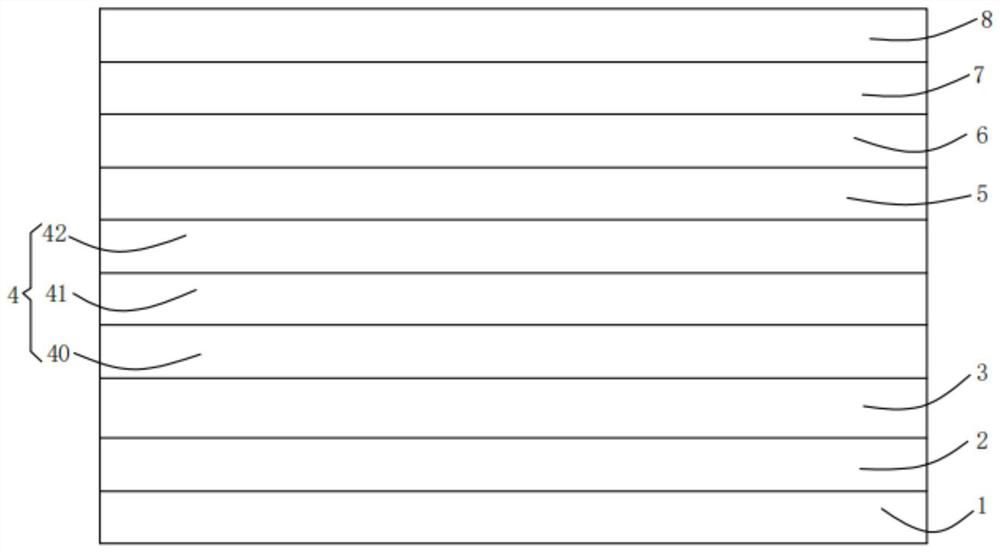
[0026] see figure 1 , is the epitaxial wafer provided in the first embodiment of the present invention, the epitaxial wafer includes a Si substrate 1, an AlN nucleation layer 3, a high resistance buffer layer 4, a GaN channel layer 5, an AlN insertion layer 6, The AlGaN barrier layer 7 and the GaN cap layer 8, and the high-resistance buffer layer 4 include a first carbon-doped AlGaN layer 40, a second carbon-doped AlGaN layer 41 and a third carbon-doped AlGaN layer 42 that are stacked in sequence. The carbon-doped AlGaN layer 40 is arranged on the side close to the AlN nucleation layer 3;

[0027] The doping concentration of the first carbon-doped AlGaN layer 40 is uniformly graded from high to low, the doping concentration of the second carbon-doped AlGaN layer 41 is constant, and the doping concentration of the third carbon-doped AlGaN layer 42 is given by Low to high uniform gradient.

[0028]It can be understood that by arranging a plurality of carbon-doped AlGaN buffer ...

Embodiment 2

[0033] see figure 2 , is the epitaxial wafer growth method provided in the second embodiment of the present invention, used for growing the epitaxial wafer in the above-mentioned first embodiment, the method includes steps S20-S21:

[0034] Step S20, providing a Si substrate, and pre-spreading an Al layer on the Si substrate;

[0035] Among them, an Al layer is pre-laid on the substrate, which can inhibit the interface reaction between the Si substrate and the epitaxial layer. Specifically, the growth temperature of the pre-laid Al layer is 1000-1100 °C, the pressure is 40-70 mbar, and the The flow rate of the incoming Al source is 50-200 sccm.

[0036] In addition, in order to improve the growth effect of the epitaxial wafer, in some optional embodiments of the present invention, the providing a Si substrate, and before the step of pre-spreading an Al layer on the Si substrate, further includes:

[0037] The Si substrate is deoxidized at a chamber temperature of 1000-1200°...

Embodiment 3

[0044] The third embodiment of the present invention provides a high electron mobility transistor, including the epitaxial wafer in the above-mentioned first embodiment, and the epitaxial wafer can be obtained by epitaxial growth by the epitaxial growth method in the above-mentioned second embodiment.


PUM

PropertyMeasurementUnit
thicknessaaaaaaaaaa
thicknessaaaaaaaaaa
thicknessaaaaaaaaaa

Abstract

The invention provides an epitaxial wafer, an epitaxial wafer growth method and a high electron mobility transistor, the epitaxial wafer comprises a Si substrate, an AlN nucleating layer, a high-resistance buffer layer, a GaN channel layer, an AlN insertion layer, an AlGaN barrier layer and a GaN cap layer which are stacked in sequence, the high-resistance buffer layer comprises a first carbon-doped AlGaN layer, a second carbon-doped AlGaN layer and a third carbon-doped AlGaN layer which are stacked in sequence, and the first carbon-doped AlGaN layer, the second carbon-doped AlGaN layer and the third carbon-doped AlGaN layer are stacked in sequence. The first carbon-doped AlGaN layer is arranged on one side close to the AlN nucleating layer; wherein the doping concentration of the first carbon-doped AlGaN layer is uniformly and gradually changed from high to low, the doping concentration of the second carbon-doped AlGaN layer is constant, and the doping concentration of the third carbon-doped AlGaN layer is uniformly and gradually changed from low to high. Compared with the prior art, the epitaxial wafer provided by the invention not only can realize high resistance, but also has very high crystal quality.

Description

technical field [0001] The invention relates to the technical field of semiconductors, in particular to an epitaxial wafer, an epitaxial wafer growth method and a high electron mobility transistor. Background technique [0002] As a third-generation semiconductor material, GaN-based materials have the advantages of large band gap, high electron saturation drift speed, good chemical stability, radiation resistance and high temperature resistance, and easy formation of heterojunctions. , The material of choice for radiation-hardened High Electron Mobility Transistor (HEMT) structures. On the other hand, due to the high carrier concentration and electron mobility of GaN-based heterostructures, its on-resistance is small, and the advantages of its large band gap make it able to withstand high operating voltages. Therefore, GaN-based high electron mobility transistors are also suitable for applications such as high-temperature, high-frequency, high-power devices, and low-loss sw...

Claims


Application Information

Patent Timeline
Patent Type & Authority Applications(China)
IPC IPC(8): H01L29/778C30B23/02C30B25/18C30B29/40H01L21/335H01L29/20H01L29/207
CPCH01L29/66462H01L29/7783H01L29/2003H01L29/207C30B23/02C30B25/183C30B29/403
Inventor 胡加辉刘春杨金从龙顾伟
Owner JIANGXI ZHAO CHI SEMICON CO LTD
Learn More