A light-emitting diode epitaxial wafer and its manufacturing method
A technology of light-emitting diodes and epitaxial wafers, which is applied to electrical components, circuits, semiconductor devices, etc., can solve the problems of increasing non-radiative recombination of carriers, affecting antistatic ability, and reducing internal quantum efficiency, so as to improve the quality of epitaxial crystals, Effects of improving internal quantum efficiency and antistatic ability, and improving warpage
- Summary
- Abstract
- Description
- Claims
- Application Information
AI Technical Summary
Problems solved by technology
Method used
Image
Examples
Embodiment 1
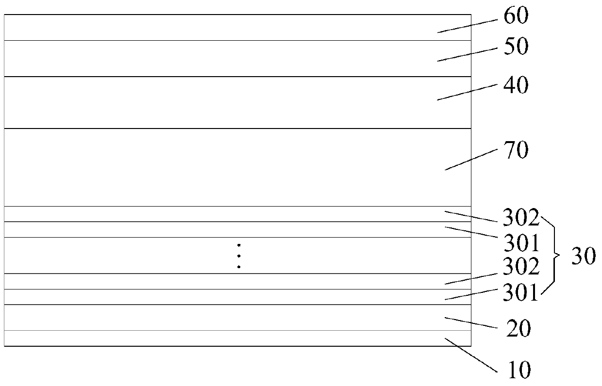
[0022] An embodiment of the present invention provides an LED epitaxial wafer, see figure 1 , the epitaxial wafer includes a substrate (not shown), a buffer layer 10 , a 3D growth layer 20 , a 2D leveling layer 30 , an N-type layer 40 , a multi-quantum well layer 50 and a P-type layer 60 .
[0023] Wherein, the 2D leveling layer 30 includes several alternately grown first sub-layers 301 and second sub-layers 302 . One of the first sublayers 301 is in direct contact with the 3D growth layer 20 . The number of first sub-layers 301 is not less than 2 and is the same as the number of second sub-layers 302 . The first sub-layer 301 is made of undoped Al x Ga 1-x N, the second sub-layer 302 is made of undoped GaN, 0.5≤x<1.
[0024] Wherein, the thickness of the first sub-layer 301 may be in the order of nanometers, and the thickness of the second sub-layer 302 may be in the order of nanometers or in the order of microns. In the first implementation of this embodiment, the 2D le...
Embodiment 2
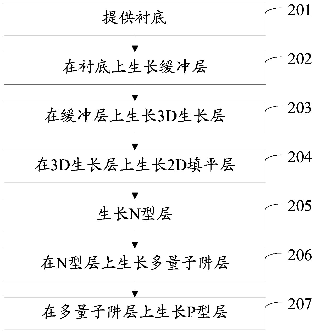
[0038] An embodiment of the present invention provides a method for manufacturing a light-emitting diode epitaxial wafer, see figure 2 , the method flow includes:
[0039] In step 201, a substrate is provided.
[0040] The substrate layer can be a sapphire substrate, or a Si substrate and a SiC substrate.
[0041] This step 201 also includes cleaning the surface of the substrate. When implemented, the substrate was heat-treated at 1100° C. for 8 minutes in an H2 atmosphere to clean the surface.
[0042] In step 202, a buffer layer is grown on the substrate.
[0043] When implemented, a layer of GaN with a thickness of 30nm is grown on the cleaned substrate at a temperature of 540°.
[0044] In step 203, a 3D growth layer is grown on the buffer layer.
[0045] When it is realized, the temperature is raised from 540°C to 1040°C, and a layer of non-doped GaN with a thickness of 0.5um is grown on the buffer layer.
[0046] In step 204, a 2D leveling layer is grown on the 3D...
PUM
 Abstract
Description
Claims
Application Information
 - R&D
- Intellectual Property
- Life Sciences
- Materials
- Tech Scout
- Unparalleled Data Quality
- Higher Quality Content
- 60% Fewer Hallucinations
Browse by: Latest US Patents, China's latest patents, Technical Efficacy Thesaurus, Application Domain, Technology Topic, Popular Technical Reports.
© 2025 PatSnap. All rights reserved.Legal|Privacy policy|Modern Slavery Act Transparency Statement|Sitemap|About US| Contact US: help@patsnap.com


