
Buried non-oxidation aperture VCSEL epitaxial structure and preparation process thereof

An epitaxial structure, non-oxidative technology, used in laser parts, semiconductor lasers, electrical components, etc., can solve the problems of maximum output power and modulation bandwidth limitations, different thermal expansion coefficients, and difficult to control the lateral geometry and size of the oxidized aperture. Achieves effects that contribute to bandwidth and high-speed modulation, no thermal expansion coefficient differences, excellent electrical confinement

Pending Publication Date: 2022-08-05
福建慧芯激光科技有限公司
View PDF1 Cites 0 Cited by
  • Summary
  • Abstract
  • Description
  • Claims
  • Application Information

AI Technical Summary

Problems solved by technology

However, the thermal conductivity of the aluminum oxide layer (0.7W / (m•K)) is lower than that of semiconductors (about 20-50W / (m•K)), which reduces the heat conduction inside the chip, resulting in increased thermal resistance
Therefore, the maximum output power of oxide-aperture VCSELs as well as the modulation bandwidth are fundamentally limited due to early thermal roll-off
In addition, the oxide layer is closely adjacent to the active area. Due to the difference in thermal expansion coefficient, internal strain is formed when the chip is working, and the internal temperature rises. The strain field will push point defects and dislocations to migrate to the active area, which will eventually lead to chip failure. reduce the reliability of the chip
[0004] From the perspective of manufacturing yield, during the oxidation process, point defects and dislocations will be generated at the interface between the oxide layer and the semiconductor, and the thermal expansion coefficients of the oxide layer and the semiconductor are different, which makes the oxidation process very difficult to control, and the process window is ultra-narrow. The oxide layer-semiconductor interface is prone to cracking or peeling off after the oxidation process
In addition, the lateral geometry and size of the oxidation pores are difficult to control and lead to variations in the size of the oxidation pores within and between sheets
In the current mature commercial manufacturing process, the absolute variation of the oxide pore diameter within and between the wafers is at least 1 μm, which limits the manufacturing yield, especially the manufacturing yield of small-aperture chips
Therefore, VCSELs with traditional oxidized apertures face many problems in the actual production environment: laser performance and reliability issues related to heat conduction; manufacturability issues related to the controllability of oxidized pores
[0006] The patent buries II-VI compound semiconductors around columnar III-V surface-emitting semiconductors to achieve optical and electrical confinement
The growth of II-VI compounds on III-V semiconductors belongs to heteroepitaxy, which is difficult and can produce at least 1e5 / cm -2 The defect density cannot be used as epitaxial wafers for laser chips in high-reliability fields such as communications
At the same time, since the current needs to be injected from the top contact layer to the slender column of the active area, this kind of VCSEL will have a much higher resistance than the traditional oxide aperture VCSEL, thus affecting the performance of the VCSEL

Method used


Image

  • Buried non-oxidation aperture VCSEL epitaxial structure and preparation process thereof
  • Buried non-oxidation aperture VCSEL epitaxial structure and preparation process thereof
  • Buried non-oxidation aperture VCSEL epitaxial structure and preparation process thereof

Examples


Embodiment Construction

[0032] The invention will be further described below with reference to the accompanying drawings and specific embodiments.

[0033] It should be noted that, the descriptions in the description and drawings given in the various embodiments of the present invention are only schematic and do not represent all specific structures.

[0034] The structures, proportions, sizes, etc. shown in the drawings attached in this specification are only used to cooperate with the contents disclosed in the specification, so as to be understood and read by those who are familiar with the technology, and are not used to limit the conditions for the implementation of the present invention. , so it has no technical substantive significance, any modification of the structure, the change of the proportional relationship or the adjustment of the size, without affecting the effect that the present invention can produce and the purpose that can be achieved, should fall within the scope of the present inv...


PUM

PropertyMeasurementUnit
thicknessaaaaaaaaaa
thicknessaaaaaaaaaa
thicknessaaaaaaaaaa

Abstract

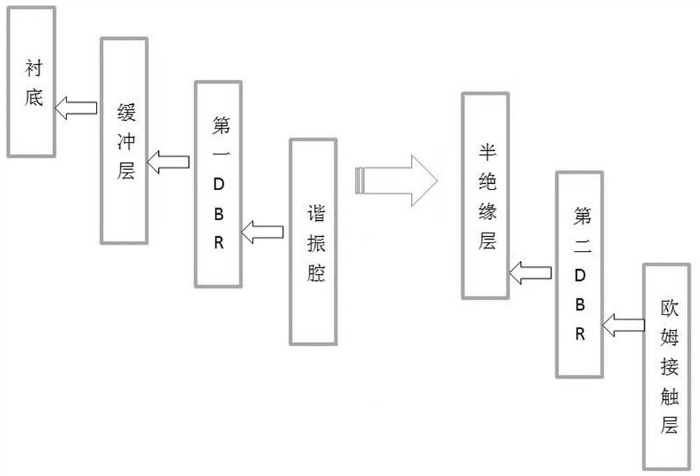
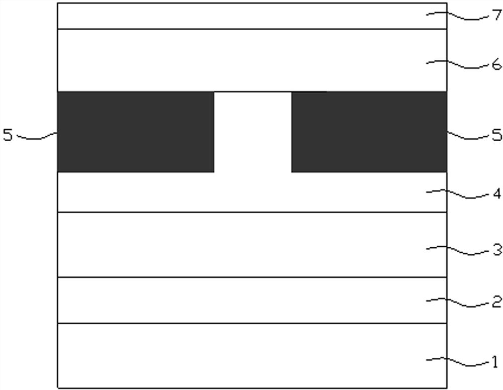
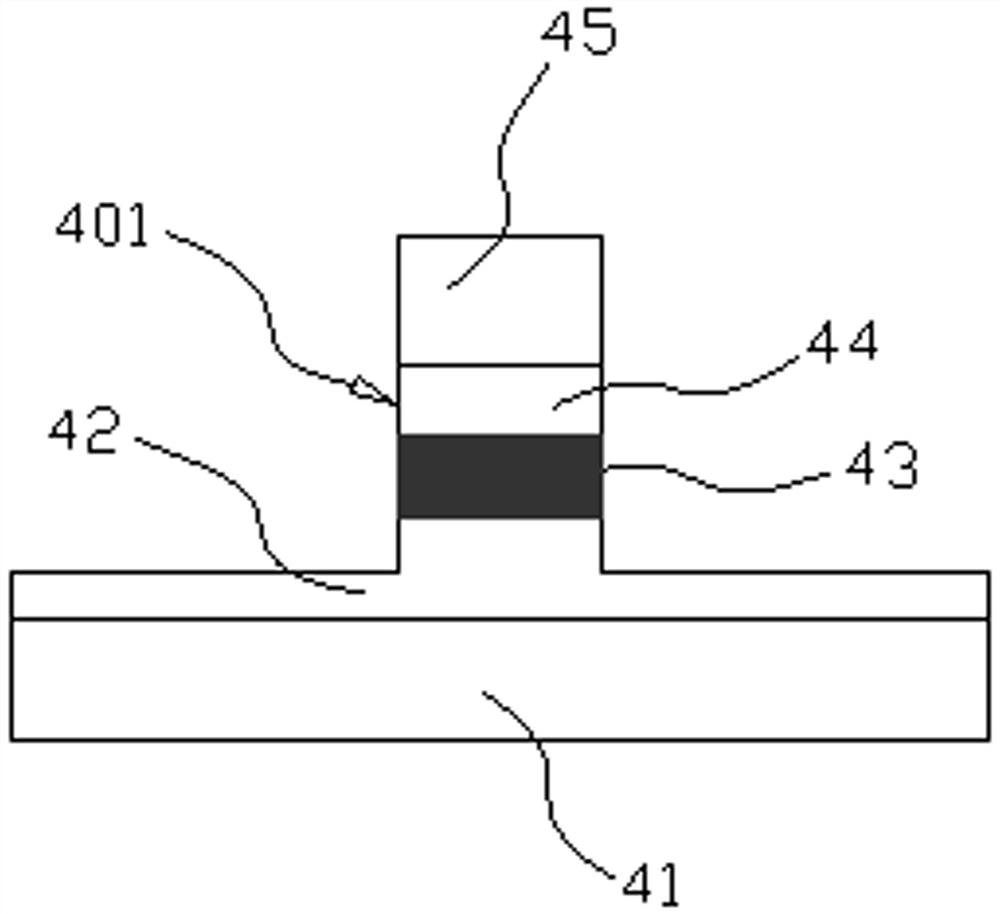
The invention provides an epitaxial structure of a buried non-oxidation aperture VCSEL, and belongs to the technical field of novel semiconductor lasers. A metal organic chemical vapor deposition (MOCVD) buffer layer, a first distributed Bragg reflection layer, a resonant cavity, a second distributed Bragg reflection layer and an ohmic contact layer are sequentially arranged on a substrate, and the resonant cavity, the second distributed Bragg reflection layer and the ohmic contact layer are all made of III-V group compound materials. A table board comprising a quantum well layer is formed on the top surface of the resonant cavity; the epitaxial structure further comprises a homogeneous semi-insulating layer, the homogeneous semi-insulating layer wraps the peripheral surface of the mesa, and the homogeneous semi-insulating layer is an Al < x > Ga < 1-x > As layer or an InP layer. According to the invention, the homogeneous semi-insulating layer regrown by the second epitaxy is buried around the resonant cavity, the semi-insulating layer regrown by the second epitaxy and the epitaxial layer in contact with the semi-insulating layer are made of homogeneous materials, surface defects between contact interfaces are fewer, thermal expansion coefficient difference does not exist, better epitaxial crystal quality can be realized, and the reliability of the device is improved.

Description

technical field [0001] The invention relates to the technical field of semiconductor lasers, and more particularly to an epitaxial structure of a buried non-oxidized aperture VCSEL and a preparation process thereof. Background technique [0002] The thermal properties of vertical-cavity surface-emitting lasers (VCSELs) are important for realizing continuous emission of chips at room temperature. [0003] At present, most VCSEL chips adopt an oxide confinement structure, that is, a layer of AlGaAs or AlAs with a certain thickness is respectively inserted between the quantum well and the upper DBR (distributed Bragg reflector). Among them, the AlGaAs layer with high Al content is in high temperature with H 2 O reacts into primary alumina, which allows good electrical confinement due to alumina being an insulator, and at the same time, a high refractive index difference between alumina (refractive index ~1.7) and semiconductor (refractive index ~3.0) , which also provides goo...

Claims


Application Information

Patent Timeline
Patent Type & Authority Applications(China)
IPC IPC(8): H01S5/183H01S5/024H01S5/125
CPCH01S5/125H01S5/18313H01S5/02469
Inventor 鄢静舟杨奕糜东林薛婷
Owner 福建慧芯激光科技有限公司
Learn More