A light-emitting diode with high luminous efficiency
A technology of light-emitting diodes and p-electrodes, applied in electrical components, circuits, semiconductor devices, etc., can solve problems such as palliatives rather than root causes, and achieve the effects of improving luminous efficiency, reducing dislocation density, and improving the quality of epitaxial crystals
- Summary
- Abstract
- Description
- Claims
- Application Information
AI Technical Summary
Problems solved by technology
Method used
Image
Examples
Embodiment Construction
[0013] One, the manufacture method step of the present invention is as follows:
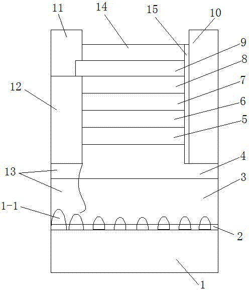
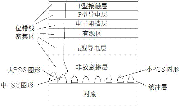
[0014] 1. Provide an epitaxial substrate. After standard masking and photolithography process, ICP etching is used to form different surface topography on the substrate surface. The PSS topography of the substrate surface topography in the p-electrode setting area is higher than that in other areas It is large and presents a certain gradual decreasing law. like figure 2 shown.
[0015] 2. Use MOCVD epitaxial equipment to sequentially form a buffer layer, an unintentionally doped layer, an n-type conductive layer (composed of four n-type conductive layers and three layers of current blocking layers), an active region, and an electron blocking layer on the epitaxial substrate. layer, p-type conductive layer, p-type ohmic contact layer.
[0016] 3. The size of the PSS surface topography passing through the substrate gradually increases in the area where the p-electrode is set, and a dislocation ...
PUM
 Abstract
Description
Claims
Application Information
 - R&D Engineer
- R&D Manager
- IP Professional
- Industry Leading Data Capabilities
- Powerful AI technology
- Patent DNA Extraction
Browse by: Latest US Patents, China's latest patents, Technical Efficacy Thesaurus, Application Domain, Technology Topic, Popular Technical Reports.
© 2024 PatSnap. All rights reserved.Legal|Privacy policy|Modern Slavery Act Transparency Statement|Sitemap|About US| Contact US: help@patsnap.com


