


Quick Research
Generate reliable direction feasibility study reports for your R&D in just a few steps.

Technical Q&A
Discover and master advanced knowledge NOW. Basics, ideas, possibilities, all at once.

Find Solutions
As an expert in R&D theories, this can generate solutions to your technical problems instantly.

Evaluate Feasibility
Analyze your overall solution with one click, know your potential R&D risks in advance.

Monitor Landscape
Get weekly tech updates, stay abreast of the latest tech innovations and key insights.
Method for realizing electronically localized passivation contacts, crystalline silicon solar cell and method for producing the same
A crystalline silicon, local technology, applied in the field of solar cell preparation, can solve the problems of difficult application of local passivation contact structure, cumbersome process steps, cumbersome preparation steps, etc., and achieve the effects of good industrialization potential, simple process and good optical performance.
- Summary
- Abstract
- Description
- Claims
- Application Information
AI Technical Summary
Problems solved by technology
Method used
Image

Examples
Embodiment 1
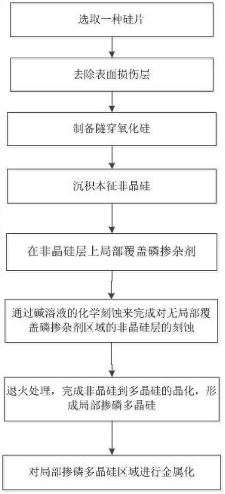
[0019] First of all, the present invention provides a method that can realize the electronic local passivation contact structure, which is combined with Embodiment 1 below figure 1 and Fig. 2, provide its main preparation process, but the following examples are only used to more clearly illustrate the technical solutions of the present invention, but not to limit the protection scope of the present invention. Embodiment 1 mainly comprises the following steps:
[0020] 1) A single crystal n-type silicon wafer or p-type silicon wafer is selected, and polycrystalline or quasi-monocrystalline silicon wafers can also be selected, but are not limited thereto. The selected silicon wafer is polished and etched with an alkaline solution (such as sodium hydroxide NaOH or potassium hydroxide KOH) or an acid solution (such as a mixed solution of nitric acid and hydrofluoric acid, etc.) to remove the damaged layer. Optionally, after removing the damaged layer, the alkali solution can be u...
Embodiment 3
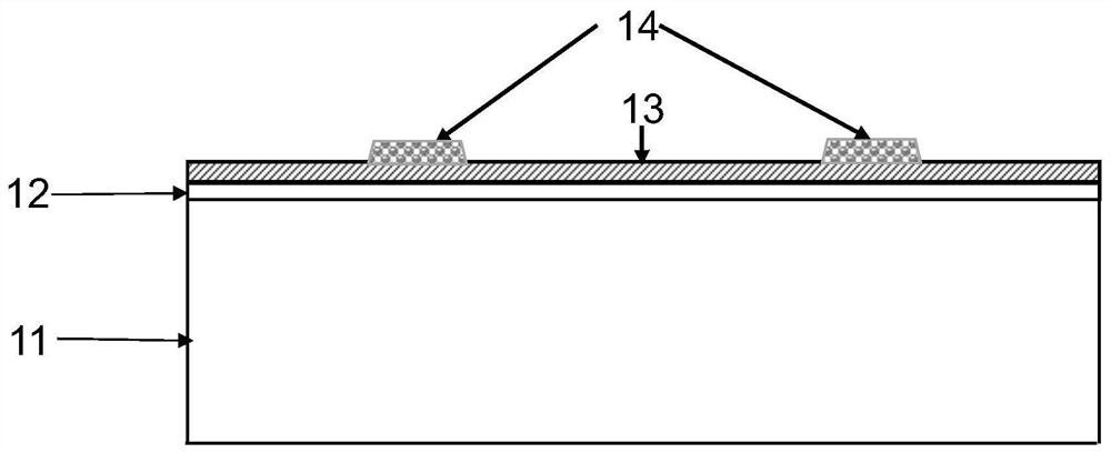
[0069] Embodiment 3 discloses a solar cell structure with an electronic local passivation contact structure and a preparation method thereof. The battery structure given in this embodiment is as follows image 3 As shown in , the front side of the cell uses a local passivation contact for electrons, and the back side of the cell uses a full-area hole passivation contact. The substrate material here is p-type single crystal silicon (or n-type single crystal silicon). The battery preparation method is as follows:
[0070] A1: Choose a 156mm*156mm (100) p-type monocrystalline silicon wafer with a resistivity of 1 Ω·cm and a thickness of 180 μm.
[0071] A2: NaOH solution is used to polish and remove the damaged layer (about 10 μm) on the surface of the p-type silicon wafer.
[0072] A3: Prepare a tunneling silicon oxide layer on the surface of the p-type silicon wafer by a thermal oxidation process, with a thickness of 1.5 nm and a refractive index of 1.46. The tunneling sili...
Embodiment 4
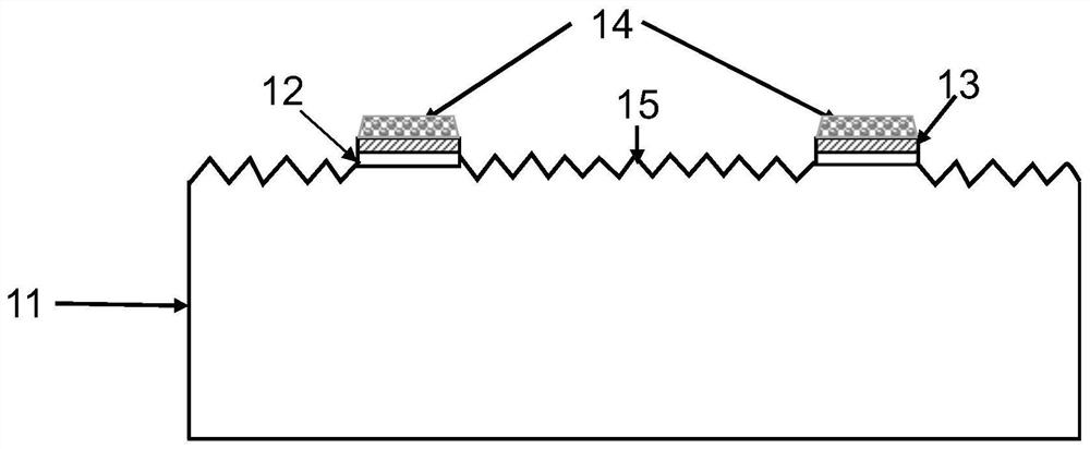
[0083] Embodiment 4 discloses another solar cell structure with electronic local passivation contact structure and its preparation method. The battery structure given in this embodiment is as follows Figure 4 As shown, the front side of the battery uses electronic local passivation contacts, and the back side of the battery uses p-type doped junctions and corresponding passivation films. In this example, the substrate material is n-type monocrystalline silicon (p-type monocrystalline silicon can also be used), and the battery preparation method is as follows:
[0084] B1: Choose a 156mm*156mm (100) n-type monocrystalline silicon wafer with a resistivity of 1 Ω·cm and a thickness of 180 μm.
[0085] B2: Polishing with NaOH solution to remove the damaged layer (about 10 μm) on the surface of the n-type silicon wafer.
[0086] B3: Perform uniform boron doping on the entire surface of the n-type silicon wafer by ion implantation combined with furnace tube annealing, and the bor...
PUM
 Abstract
Description
Claims
Application Information
 - R&D Engineer
- R&D Manager
- IP Professional
- Industry Leading Data Capabilities
- Powerful AI technology
- Patent DNA Extraction
Browse by: Latest US Patents, China's latest patents, Technical Efficacy Thesaurus, Application Domain, Technology Topic, Popular Technical Reports.
© 2024 PatSnap. All rights reserved.Legal|Privacy policy|Modern Slavery Act Transparency Statement|Sitemap|About US| Contact US: help@patsnap.com