


Quick Research
Generate reliable direction feasibility study reports for your R&D in just a few steps.

Technical Q&A
Discover and master advanced knowledge NOW. Basics, ideas, possibilities, all at once.

Find Solutions
As an expert in R&D theories, this can generate solutions to your technical problems instantly.

Evaluate Feasibility
Analyze your overall solution with one click, know your potential R&D risks in advance.

Monitor Landscape
Get weekly tech updates, stay abreast of the latest tech innovations and key insights.
Preparation method of ceramic-based electronic circuit
An electronic circuit, ceramic-based technology, applied in the directions of printed circuits, printed circuit parts, electrical components, etc., can solve the problems of reducing the preparation accuracy of electronic circuits, increasing the processing defects of electronic circuits, and not having high heat resistance, etc. Achieve excellent interface bonding, avoid over-plating problems, and ensure the effect of process stability
- Summary
- Abstract
- Description
- Claims
- Application Information
AI Technical Summary
Problems solved by technology
Method used
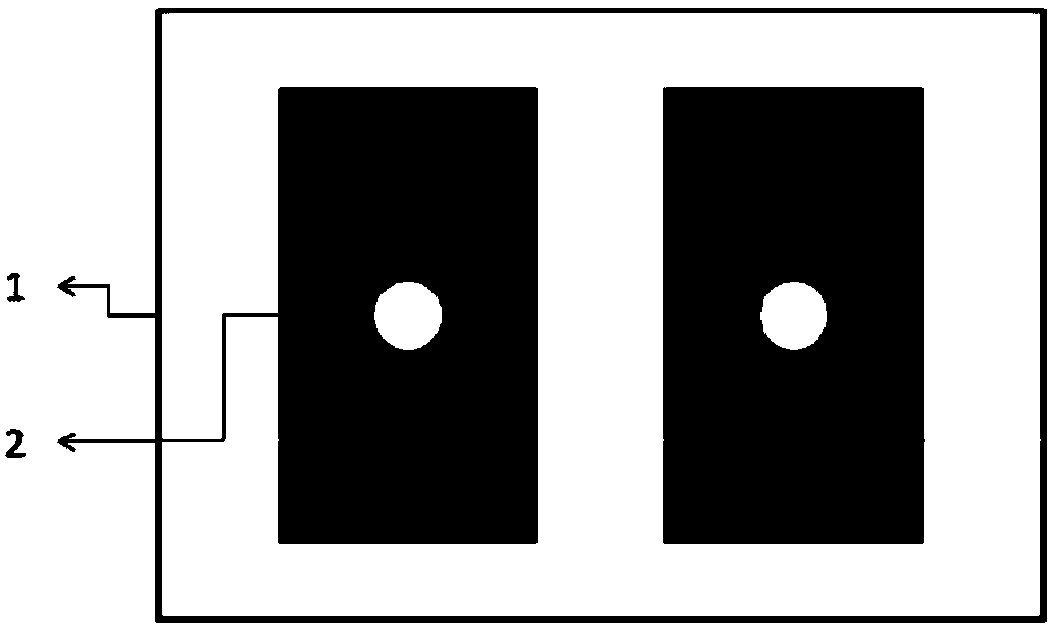
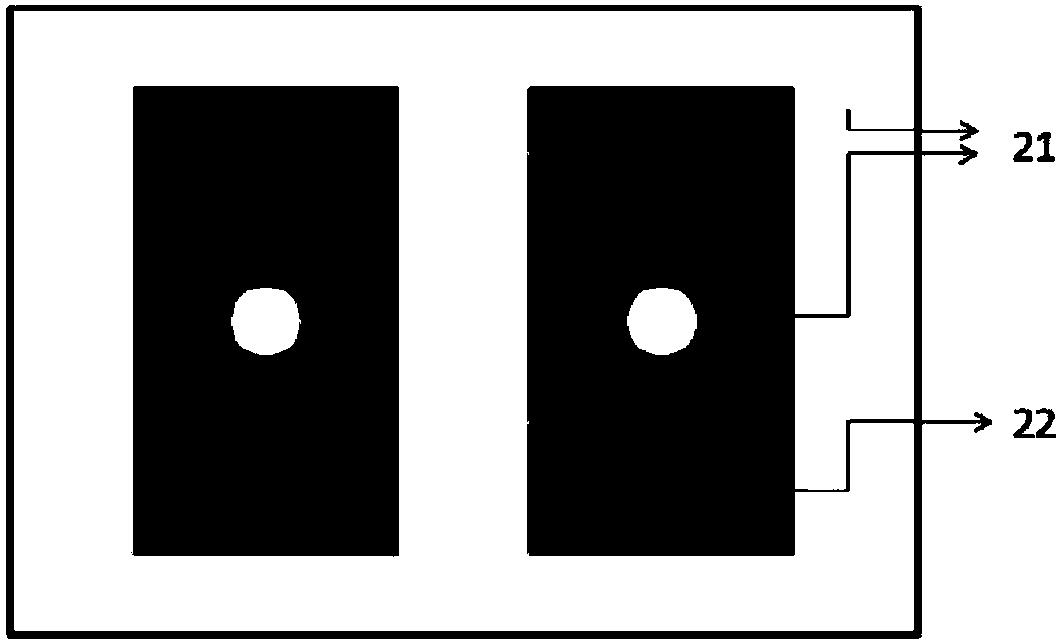
Image


Examples
Embodiment 1
[0038] A method for preparing a ceramic-based electronic circuit, comprising the following steps:
[0039] S1) Preparation of ceramic substrate: select 95 alumina powder (conventional commercially available powder is enough) as raw material, use tape casting-lamination-sintering process to prepare the required ceramic substrate, and use mechanical cutting to cut the ceramic substrate into the required size, using grinding and polishing, the surface of the ceramic substrate is processed to a roughness of 0.2u±0.05u(Ra), and the arithmetic mean deviation of the contour is Ra;
[0040] S2) Prepare the surface protective layer: select magenta: CMC=50wt%: 50wt% as mixed solute, use deionized water as diluent, configure a protective layer solution with a concentration of 5g / L, and use a spraying process to evenly coat the protective layer solution Cover the surface of the ceramic substrate described in step S1, and dry at 75°C for 1 hour; here the magenta is basic fuchsin C 20 h 2...
Embodiment 2
[0046] S10) According to the method similar to that described in Example 1, according to the ratio of alumina: zirconia: magnesia: lanthanum manganate = 12wt%: 80wt: 5wt%: 3wt% as raw material, prepare a ceramic substrate; and use grinding and polishing process, the surface roughness of the ceramic substrate is controlled in several different specifications, and the specific statistics are shown in Table 1:
[0047] Table 1 Several ceramic substrates with different surface roughness
[0048] Specification
Surface Processing Process
Surface roughness range Ra / um
A
coarse grinding
0.55~0.79
B
coarse grinding + fine grinding
0.05~0.09
C
Coarse Grinding + Rough Polishing
0.03~0.05
D
Coarse grinding + rough polishing + fine polishing
0.02~0.03
[0049] S20) Prepare the surface protection layer: configure two different surface protection layer solutions according to the statistics in Table 2;
[0050] Table 2...
PUM
| Property | Measurement | Unit |
|---|---|---|
| concentration | aaaaa | aaaaa |
Abstract
Description
Claims
Application Information
 - R&D Engineer
- R&D Manager
- IP Professional
- Industry Leading Data Capabilities
- Powerful AI technology
- Patent DNA Extraction
Browse by: Latest US Patents, China's latest patents, Technical Efficacy Thesaurus, Application Domain, Technology Topic, Popular Technical Reports.
© 2024 PatSnap. All rights reserved.Legal|Privacy policy|Modern Slavery Act Transparency Statement|Sitemap|About US| Contact US: help@patsnap.com