Apparatus for fabricating flat panel display, and apparatus and method for detecting quantity of static electricity thereof
- Summary
- Abstract
- Description
- Claims
- Application Information
AI Technical Summary
Benefits of technology
Problems solved by technology
Method used
Image
Examples
first embodiment
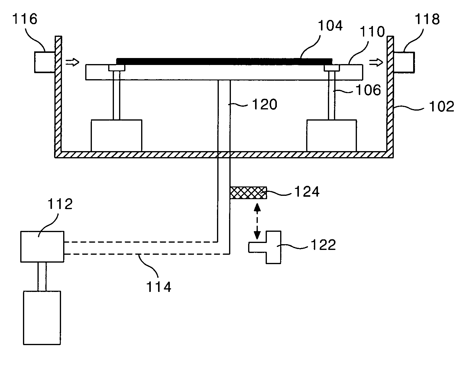
[0034] A process of detecting the quantity of static electricity on the substrate using the fabricating apparatus of the flat panel display device according to the present invention is as follows. After a deposition process is complete, the susceptor 110 is lowered so that the lift pins are 106 are deployed to raise the substrate 104 off of the susceptor 104. The susceptor 110 is affixed to a supporting stand 120. The susceptor 110 is moved in a vertical direction by a timing belt 114, which is connected to the supporting stand 120, and a motor 112, which drives the time belt 114.
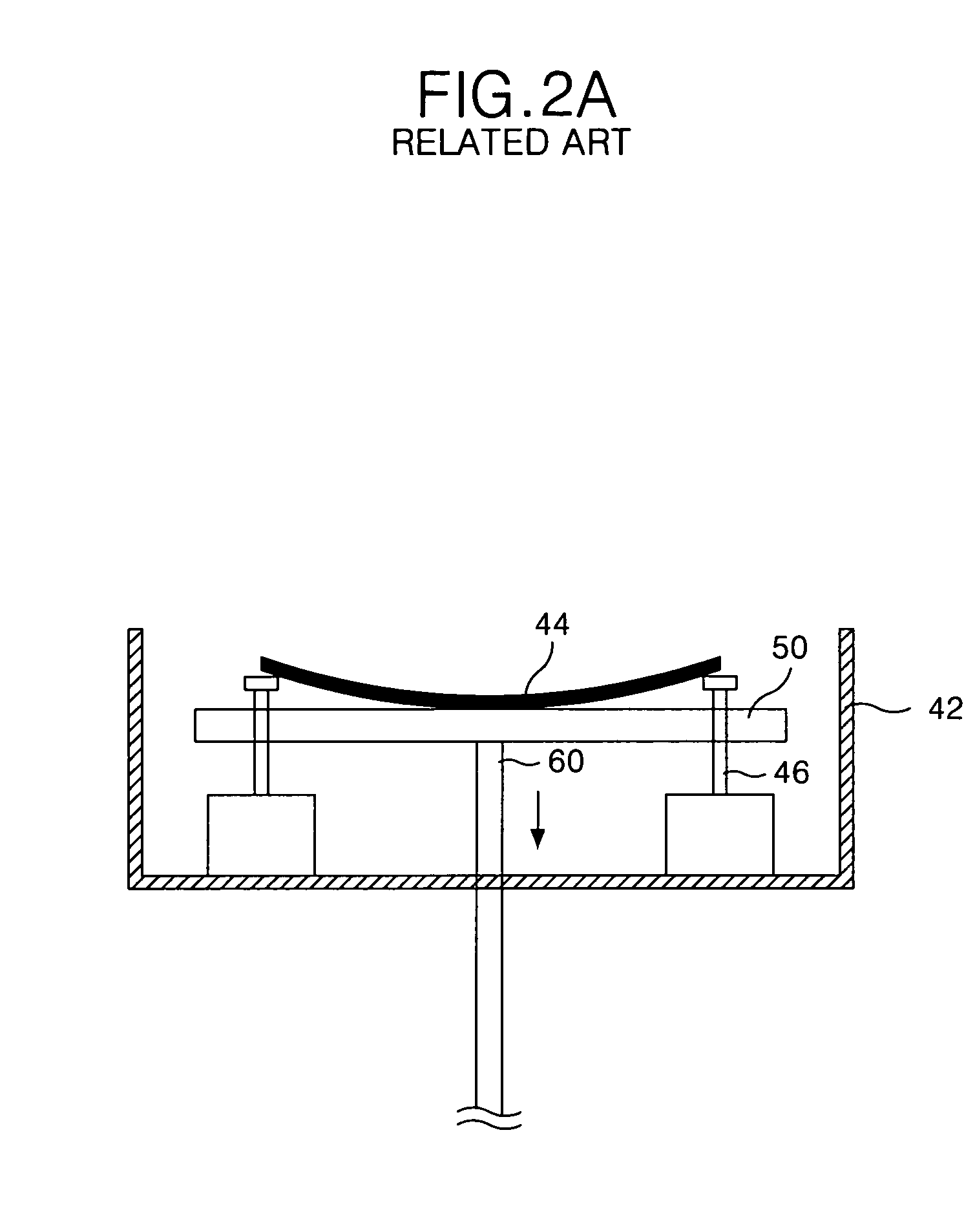
[0035] A static electric charge generated between the substrate 104 and the susceptor 110 by an RF discharge during the deposition process prevents the substrate 104 from properly separating from the susceptor 110 due to static electricity holding the middle part of the substrate where no lift pins are located when the lift pins are deployed and thus the substrate 104 is bent as a result. To remove the stat...
second embodiment
[0050] A process of detecting the static electricity quantity on substrate by use of the fabricating apparatus of the flat panel display device according to the present invention having such a configuration is as follows. The lift pins 306 ascend upward by a motor 312 after the deposition process is completed so that the substrate 304 can be positioned for a subsequent process by a robot arm (not shown).
[0051] The susceptor 310 is affixed to a supporting stand 320 while the lift pins 306 ascend to lift the substrate 304 such that there is a space between the susceptor 310 and the substrate 304 into which the robot arm can enter. A static electric charge placed on the substrate 304 by the RF discharge during the deposition process such that the substrate 304 can not be easily separated from the susceptor 310 in the middle part of the substrate 304 where no lift pins 306 are located when the lift pin ascends. Thus, the substrate 304 is bent as a result. To remove the static electricit...
PUM
| Property | Measurement | Unit |
|---|---|---|
| Distance | aaaaa | aaaaa |
Abstract
Description
Claims
Application Information
 - R&D
- Intellectual Property
- Life Sciences
- Materials
- Tech Scout
- Unparalleled Data Quality
- Higher Quality Content
- 60% Fewer Hallucinations
Browse by: Latest US Patents, China's latest patents, Technical Efficacy Thesaurus, Application Domain, Technology Topic, Popular Technical Reports.
© 2025 PatSnap. All rights reserved.Legal|Privacy policy|Modern Slavery Act Transparency Statement|Sitemap|About US| Contact US: help@patsnap.com


