Integrated energy supply product, preparation method thereof and device
A product and energy technology, which is applied in the field of energy supply products and its preparation, can solve the problems of small bendability, human injury, and heavy weight, and achieve the effects of improved stability and safety, safe and stable work, and low design difficulty
- Summary
- Abstract
- Description
- Claims
- Application Information
AI Technical Summary
Problems solved by technology
Method used
Image
Examples
Embodiment 1
[0058] production material:
[0059] GaAs substrate, Ge substrate, aluminum-plastic film, flexible PET or PEN film, EVA glue, arsine (AsH 3 ), phosphine (PH 3 ), trimethylaluminum (TMAl), trimethylgallium (TMGa), trimethylindium (TMIn), silane (SiH4), H 2 S, diethyl zinc (DEZn), tetrachloromethane (CCl 4 ), etc.; metal foils such as stainless steel, copper, silver, etc.; targets such as LiCoO 2 , Li 3 PO 4 , Li 2 MnO 4 , Cu, Ag, Au, etc.; evaporation sources such as Li particles, Au particles, PEN organic evaporation sources, etc.
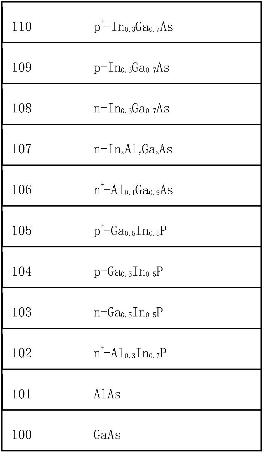
[0060] Preparation of triple-five double-junction batteries:
[0061] S1. GaAs substrate cleaning and drying. Use acetone or alcohol with ultrasonic cleaning, and then put it in the dryer to dry.
[0062] MOCVD (metal organic chemical vapor deposition) method is used to epitaxially grow sacrificial layer, buffer layer, emitter layer, tunnel junction, window layer, etc. on the GaAs substrate in sequence. The precursor gas introduced in the...
Embodiment 2
[0090] Preparation of triple-five double-junction batteries:
[0091] Step 1. Use Ge substrate to reduce cost. MOCVD (metal organic chemical vapor deposition) method is used to epitaxially grow sacrificial layer, buffer layer, emitter layer, tunnel junction, window layer, etc. on the substrate in sequence. The precursor gas introduced in the MOCVD process is arsine (AsH 3 ), phosphine (PH 3 ), trimethylaluminum (TMAl), trimethylgallium (TMGa), trimethylindium (TMIn) and other gases. Doping with tetrabromomethane (CBr 4 ) and H 2 S.
[0092] In the epitaxial layer structure, the thickness of the substrate is 160 μm, and the thickness of the sacrificial layer is 80 nm; n-type Al 0.3 In 0.7 The thickness of the P window layer is 50nm, and the doping concentration is 1×10 19 cm -3 ; n-type Ga 0.5 In 0.5 P emitter region, thickness 50nm, p-type Ga 0.5 In 0.5 P base region, thickness 50nm, p-type Ga 0.5 In 0.5 P tunnel junction, thickness 30nm, n-type Al 0.1 Ga 0.9 A...
Embodiment 3
[0098] The flexible thin-film III-V solar cell has a photoelectric conversion efficiency of up to 29%. Embodiment 3 Preparation of all-solid-state thin-film lithium battery
[0099] In this embodiment, in step 1, a layer of SiO with a thickness of 100 nm is plated on the copper foil. 2 film.
[0100] Step 3 The magnetron sputtering chamber selects LiMn 2 o 4, deposited with a thickness of 80nm to form the positive electrode of a lithium battery. After the deposition, the sample stage was heated to 400°C-500°C, and annealed for about 15 minutes to obtain a film with uniform grain size, and then cooled naturally.
[0101] In step 5, the thickness of the LiPON electrolyte film is 100nm.
[0102] Other operations are the same as in Example 1.
[0103] The present invention adopts the integrated integration of thin-film solar cells and thin-film lithium batteries to realize soft, bendable and easy-to-carry batteries, making electronic products lighter in weight. The third an...
PUM
| Property | Measurement | Unit |
|---|---|---|
| thickness | aaaaa | aaaaa |
| thickness | aaaaa | aaaaa |
| thickness | aaaaa | aaaaa |
Abstract
Description
Claims
Application Information
 - R&D
- Intellectual Property
- Life Sciences
- Materials
- Tech Scout
- Unparalleled Data Quality
- Higher Quality Content
- 60% Fewer Hallucinations
Browse by: Latest US Patents, China's latest patents, Technical Efficacy Thesaurus, Application Domain, Technology Topic, Popular Technical Reports.
© 2025 PatSnap. All rights reserved.Legal|Privacy policy|Modern Slavery Act Transparency Statement|Sitemap|About US| Contact US: help@patsnap.com


