Thermoelectric device and electrode thereof, and method for preparing electrode
A technology of thermoelectric devices and electrodes, which is applied to the manufacture/processing of thermoelectric device parts and thermoelectric devices, etc., which can solve the problems of decreased stability of thermoelectric devices, reduced performance of thermoelectric materials, and increased interface contact resistance, so as to improve stability , High production efficiency, small interface contact resistance
- Summary
- Abstract
- Description
- Claims
- Application Information
AI Technical Summary
Problems solved by technology
Method used
Image
Examples
preparation example Construction
[0030] Correspondingly, the embodiment of the present invention also provides a preparation method of the thermoelectric device electrode mentioned above. This preparation method comprises the steps:
[0031] S01. laying titanium-nickel alloy barrier layer powder layer, solder layer 3 and electrode layer 4 sequentially on the surface of the half-Heusler substrate;
[0032] S02. Carry out sintering treatment again.
[0033] Specifically, the half-Heusler matrix, the solder layer 3 and the electrode layer 4 in the above step S01 are all as described above, and will not be repeated here to save space. Wherein, the solder layer 3 may be a solder foil, specifically a silver-copper-zinc solder foil with a melting point of 600-800°C. The electrode layer 4 can be but not only a copper sheet.
[0034] In this step S01, after the powder layer of the barrier layer is sintered, the powder is sintered to form the barrier layer 2 contained in the electrode of the thermoelectric device de...
Embodiment 1
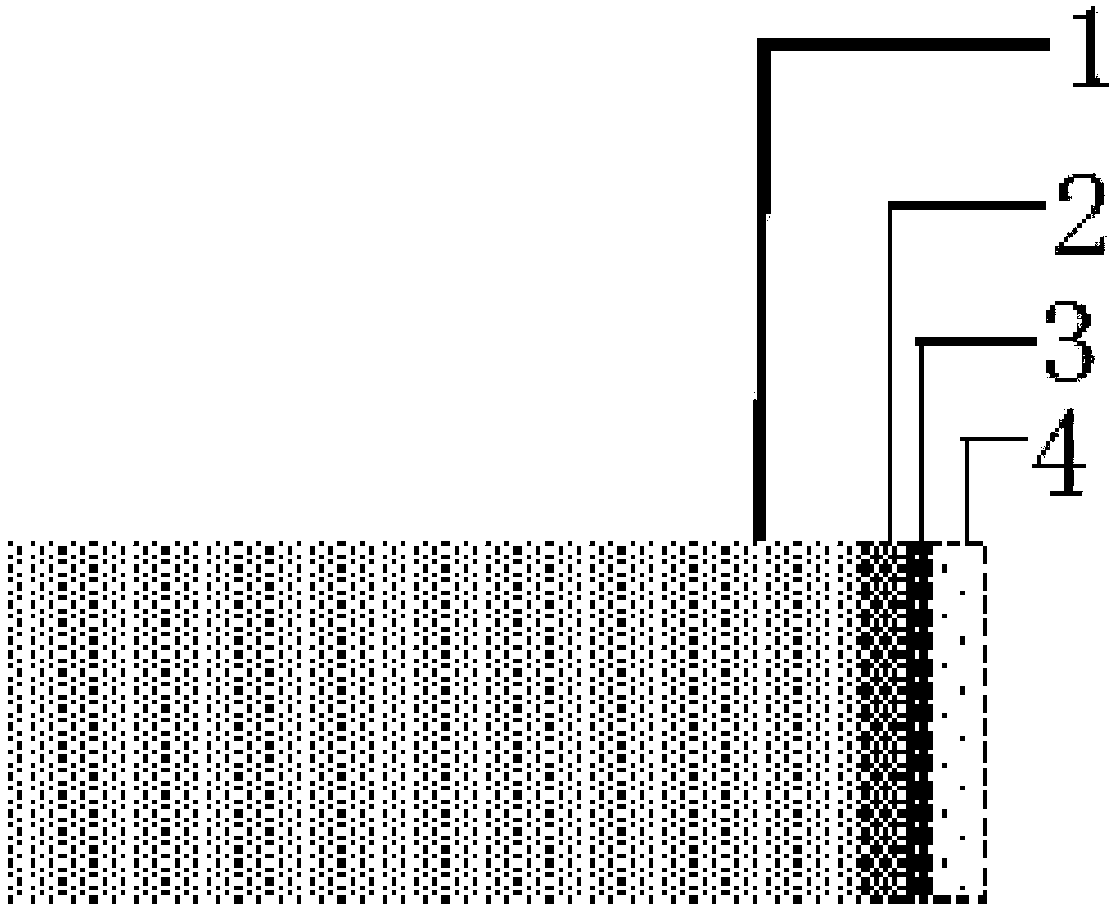
[0047] This embodiment provides a thermoelectric device electrode and a preparation method thereof. The electrode structure of the thermoelectric device is as follows figure 1 As shown, it includes a half-Heusler matrix layer 1, a barrier layer 2, a solder layer 3, and a copper electrode layer 4 stacked on the surface of the half-Heusler matrix layer 1. Wherein, the barrier layer 2 has a thickness of 0.5 mm, and the solder foil has a thickness of 0.05 mm. The thickness of the copper electrodes was 0.8 mm.
[0048] The preparation method of the thermoelectric device electrode in this embodiment is as follows:
[0049] Preparation of S11half-Heusler thermoelectric material bulk:
[0050] a Proportional weighing of the elemental elements used, arc smelting the elements other than Sb, weighing the required amount of Sb according to the obtained ingot proportioning after smelting, and grinding the above two materials to obtain a mixed powder Body; arc melting current is 150A, v...
Embodiment 2
[0060] This embodiment provides a thermoelectric device electrode and a preparation method thereof. The electrode structure of the thermoelectric device is the same as that of Example 1.
[0061] The preparation method of the thermoelectric device electrode of this embodiment is as follows:
[0062] S21 The preparation of the half-Heusler thermoelectric material block refers to S11 of Example 1; wherein, the material half-Heusler is n-type half-Heusler, and the temperature of SPS hot pressing is 850°C (n-type), and the sintering pressure is 35MPa, the highest sintering The temperature maintenance time is 10min-15min, and the cooling time is more than 25min. A graphite mold with an inner diameter of 15mm, a mold sleeve length of 40mm, a graphite indenter with an outer diameter of 14.6mm and a length of 25mm is used;
[0063] Step S12 in S22 parameter embodiment 1, wherein,
[0064] Sintering conditions: the sintering temperature of N-HH / barrier layer material is selected at 7...
PUM
| Property | Measurement | Unit |
|---|---|---|
| Thickness | aaaaa | aaaaa |
| Thickness | aaaaa | aaaaa |
| Thickness | aaaaa | aaaaa |
Abstract
Description
Claims
Application Information
 - Generate Ideas
- Intellectual Property
- Life Sciences
- Materials
- Tech Scout
- Unparalleled Data Quality
- Higher Quality Content
- 60% Fewer Hallucinations
Browse by: Latest US Patents, China's latest patents, Technical Efficacy Thesaurus, Application Domain, Technology Topic, Popular Technical Reports.
© 2025 PatSnap. All rights reserved.Legal|Privacy policy|Modern Slavery Act Transparency Statement|Sitemap|About US| Contact US: help@patsnap.com


