Light-emitting diode (LED) light source encapsulating structure special for automobile headlamp
A technology of LED light sources and automobile headlights, which is applied in the field of packaging structure of LED light sources for automobile headlights, can solve the problems of harsh headlight standards, harsh use environments, and not commonly used in automobile headlights, etc., and achieve clear Brightness cut-off line, low package thermal resistance, the effect of meeting the requirements of use
- Summary
- Abstract
- Description
- Claims
- Application Information
AI Technical Summary
Problems solved by technology
Method used
Image
Examples
Embodiment 1
[0025] Embodiments of the present invention are further described below in conjunction with the accompanying drawings:
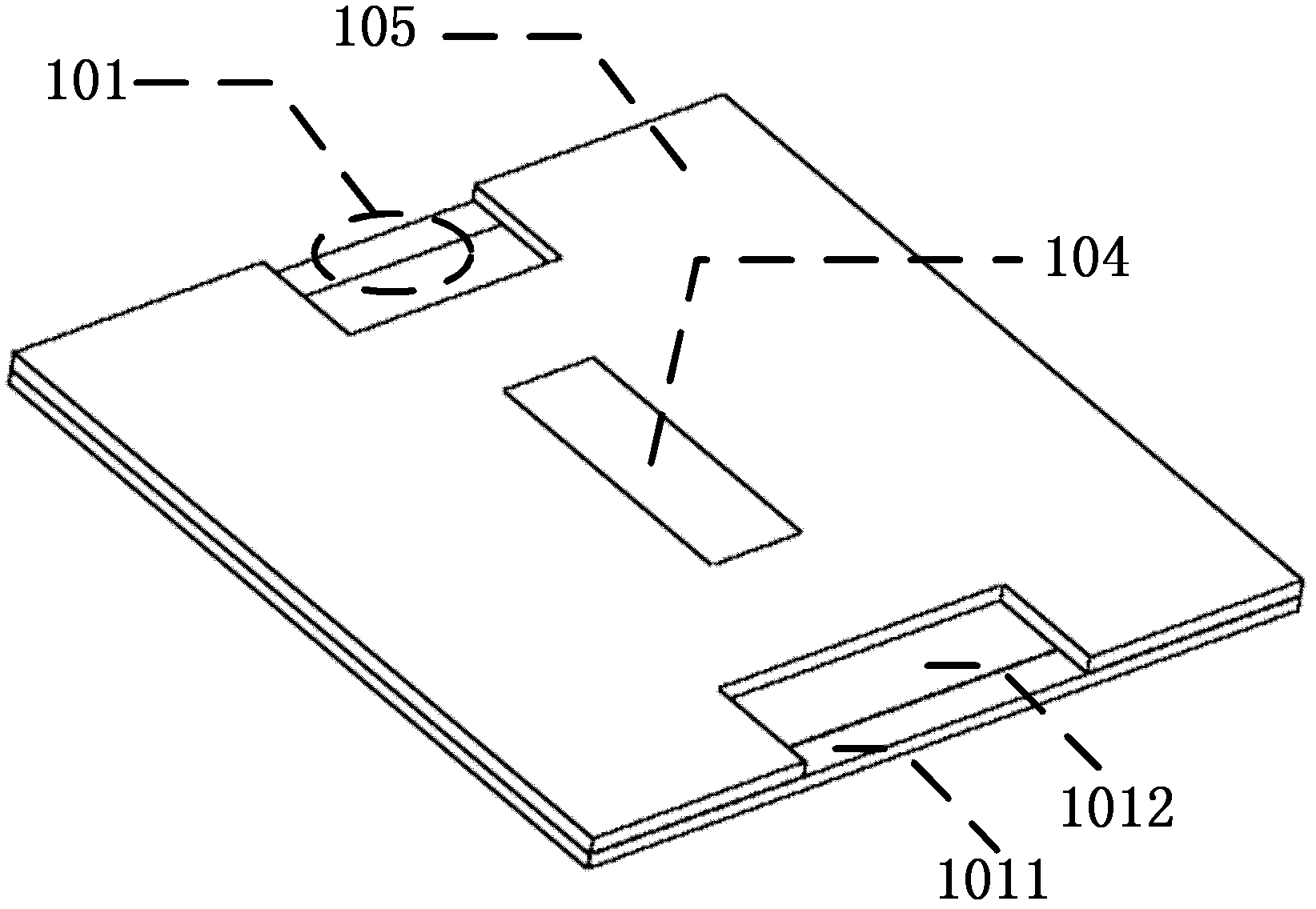
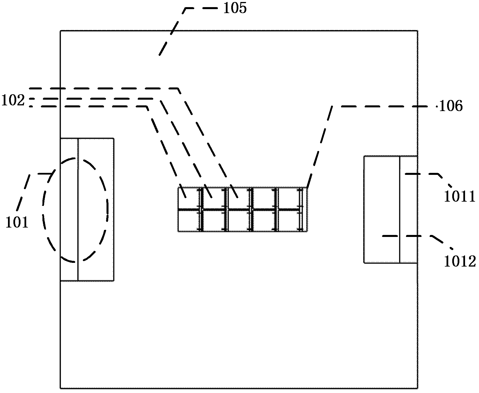
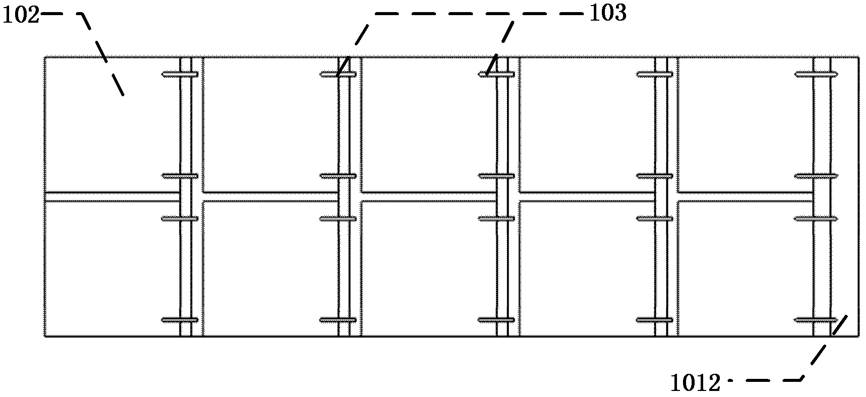
[0026] The special LED light source package for automobile headlights of the present invention comprises a metallized thin film ceramic substrate 101, and the metallized thin film ceramic substrate 101 is composed of a bottom aluminum nitride substrate 1011 and an upper layer of metallized copper layer 1012; the LED chip 102 is installed On the packaging substrate, the packaging substrate of this embodiment is a metallized thin film ceramic substrate 101, and the LED chips 102 are arranged in a rectangular shape with a plurality of high-power blue light chips. The ×5 array is arranged on the metallized thin film ceramic substrate 101, the length of the rectangular area ranges from 1.5mm to 8mm, and the width ranges from 1mm to 4mm; the gold wire 103 connects 10 LED chips in two columns in series; the phosphor layer 104 covers On the LED chip 102, the phospho...
Embodiment 2
[0028] Embodiment 2 is the same as Embodiment 1, except that the packaging substrate of this embodiment is a double-sided copper-clad ceramic substrate DBC substrate 201 with high thermal conductivity. The bottom copper clad layer 2013 is composed; the LED chip 102 is arranged on the substrate 201 by 10 square high-power blue chips in a 2×5 array; the gold wire 103 connects the 10 LED chips in two columns in series; the phosphor layer 104 covers the chip 102; the packaging cover 105 has a rectangular hole 106 in the middle, so that the chip 102 and the fluorescent layer 104 are placed in it; and the DBC substrate 201 is provided with two fixing holes 207. see Figure 4 , Figure 5 , Figure 6 , Figure 7 .
Embodiment 3
[0030] The third embodiment is the same as the second embodiment, except that the copper layer on the bottom surface of the substrate in this embodiment is a steam chamber, and the substrate 201 with the steam chamber is composed of an alumina ceramic substrate 2011, an upper copper clad layer 2012 and a steam chamber. 3013, the steam chamber 3013 contains distilled water 30131, and a temperature sensor 3014 is integrated on the substrate 201 with the steam chamber; the LED chip 102 is arranged on the substrate 301 by 10 square high-power blue light chips in a 2×5 array; gold The wire 103 connects 10 LED chips in two columns in series; the phosphor layer 104 covers the chip 102; the packaging cover sheet 105 has a rectangular hole 106 in the middle, so that the chip 102 and the phosphor layer 104 are placed in it. see Figure 8 , Figure 9 , Figure 10 .
PUM
| Property | Measurement | Unit |
|---|---|---|
| Length | aaaaa | aaaaa |
| Width | aaaaa | aaaaa |
Abstract
Description
Claims
Application Information
 - R&D
- Intellectual Property
- Life Sciences
- Materials
- Tech Scout
- Unparalleled Data Quality
- Higher Quality Content
- 60% Fewer Hallucinations
Browse by: Latest US Patents, China's latest patents, Technical Efficacy Thesaurus, Application Domain, Technology Topic, Popular Technical Reports.
© 2025 PatSnap. All rights reserved.Legal|Privacy policy|Modern Slavery Act Transparency Statement|Sitemap|About US| Contact US: help@patsnap.com


