A packaging structure and packaging process in which welding, bonding and sealing are completed simultaneously
A packaging technology and bonding technology, which is applied in the direction of electrical components, electric solid devices, circuits, etc., can solve problems such as unfavorable heat dissipation of devices, many packaging process steps, and complicated packaging structure, so as to reduce packaging costs, facilitate operation, and reduce The effect of production costs
- Summary
- Abstract
- Description
- Claims
- Application Information
AI Technical Summary
Problems solved by technology
Method used
Image
Examples
Embodiment 1
[0034] Embodiment 1: A packaging process in which welding, bonding and sealing are completed simultaneously, comprising the following steps:
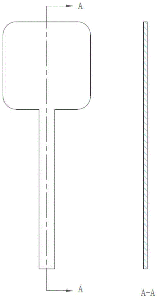
[0035] Step (1), according to the size and specification requirements of the packaged chip, punch or etch the first terminal cover 1 and the second terminal cover 2, and electroplate the Ni-Au layer on the second terminal cover 2 ;
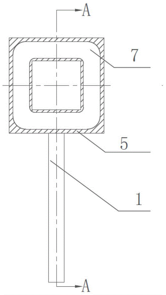
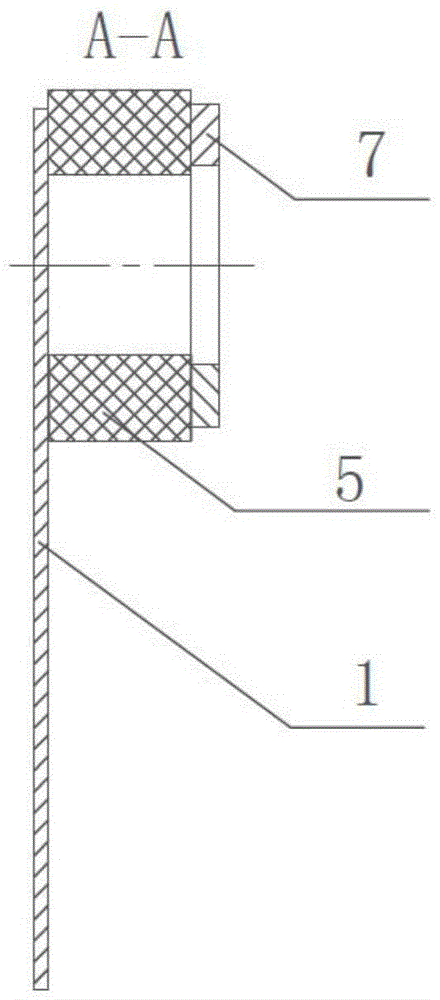
[0036] Step (2), using metallized co-firing or making porcelain parts to prepare through-cavity ceramics 5 through metallization treatment, and then electroless nickel plating on the upper and lower end faces of the prepared through-cavity ceramics 5; Provide better wettability for brazing;
[0037] In step (3), the first lead-out cover plate 1 and the sealing ring 7 are respectively brazed to the lower end surface and the upper end surface of the through-cavity ceramics with silver-copper solder, and electroplated with Ni-Au or Ni-Ag protective coating.
[0038] Step (4), welding one terminal of the two-...
Embodiment 2
[0042] Embodiment 2: a packaging process in which welding, bonding and sealing are completed simultaneously, comprising the following steps:
[0043] Step (1), according to the size and specification requirements of the packaged chip, punch or etch the first terminal cover 1 and the second terminal cover 2, and electroplate the Ni-Au layer on the second terminal cover 2 ;
[0044] Step (2), using metallized co-firing or making porcelain parts to prepare through-cavity ceramics 5 through metallization treatment, and then electroless nickel plating on the upper and lower end faces of the prepared through-cavity ceramics 5; Provide better wettability for brazing;
[0045] Step (3), brazing the first lead-out cover plate 1 and the sealing ring 7 to the lower end surface and the upper end surface of the through-cavity ceramics respectively by silver-copper solder, and electroplating a Ni-Au or Ni-Ag protective coating;
[0046] Step (4), first place the SAC305 solder 4 on the fir...
PUM
 Abstract
Description
Claims
Application Information
 - R&D
- Intellectual Property
- Life Sciences
- Materials
- Tech Scout
- Unparalleled Data Quality
- Higher Quality Content
- 60% Fewer Hallucinations
Browse by: Latest US Patents, China's latest patents, Technical Efficacy Thesaurus, Application Domain, Technology Topic, Popular Technical Reports.
© 2025 PatSnap. All rights reserved.Legal|Privacy policy|Modern Slavery Act Transparency Statement|Sitemap|About US| Contact US: help@patsnap.com


