Manufacturing method of led packaging structure

A technology of LED packaging and manufacturing method, applied in electrical components, circuits, semiconductor devices, etc., can solve the problem that the thermal resistance from chip to circuit board cannot be effectively reduced, and achieve the effect of reducing thermal resistance, improving quality, and saving production costs

Active Publication Date: 2017-12-05
厦门多彩光电子科技有限公司
View PDF3 Cites 0 Cited by
  • Summary
  • Abstract
  • Description
  • Claims
  • Application Information

AI Technical Summary

Problems solved by technology

It can be seen that because the existing flip-chip LED chip packaging technology is to fix the LED chip on the bracket or the substrate, the heat dissipation needs to be conducted by the bracket or the substrate and then transferred to the soldered circuit board. The thermal resistance between the chip and the circuit board cannot be solved. effectively reduce

Method used


Image

  • Manufacturing method of led packaging structure
  • Manufacturing method of led packaging structure
  • Manufacturing method of led packaging structure

Examples


Embodiment Construction

[0025] To further illustrate the various embodiments, the present invention is provided with accompanying drawings. These drawings are a part of the disclosure of the present invention, which are mainly used to illustrate the embodiments, and can be combined with related descriptions in the specification to explain the operating principles of the embodiments. With reference to these contents, those skilled in the art should understand other possible implementations and advantages of the present invention. Components in the figures are not drawn to scale, and similar component symbols are generally used to denote similar components.

[0026] The present invention will be further described in conjunction with the accompanying drawings and specific embodiments.

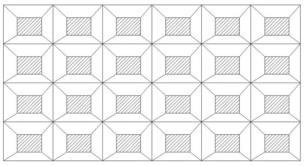
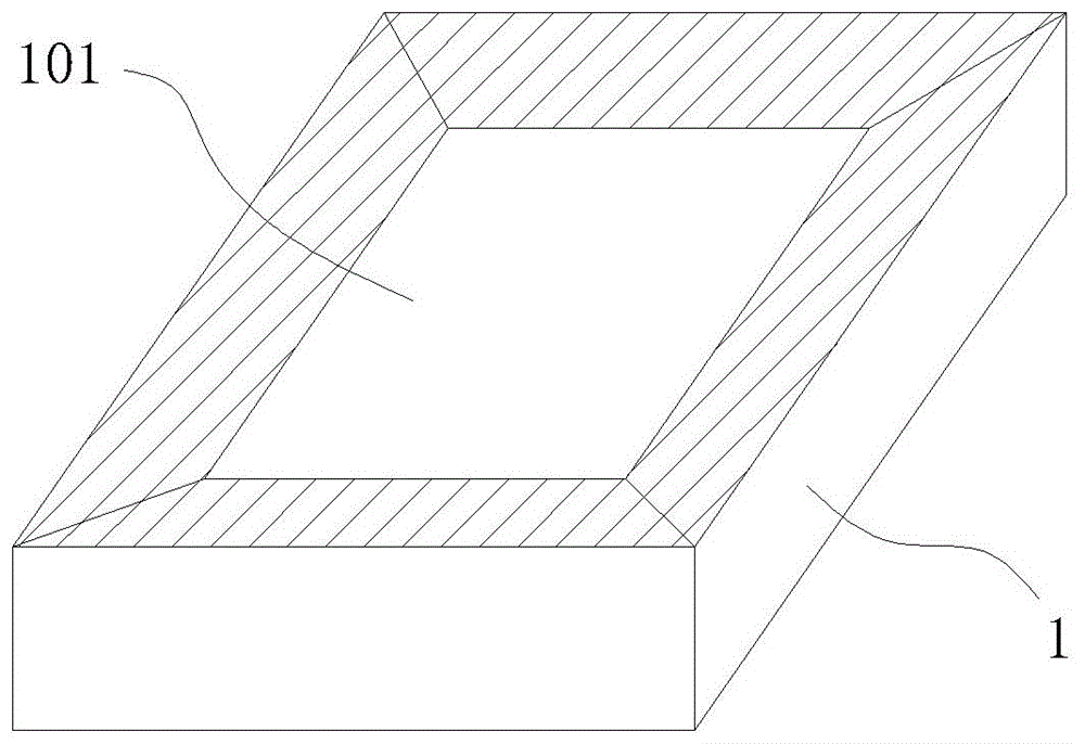
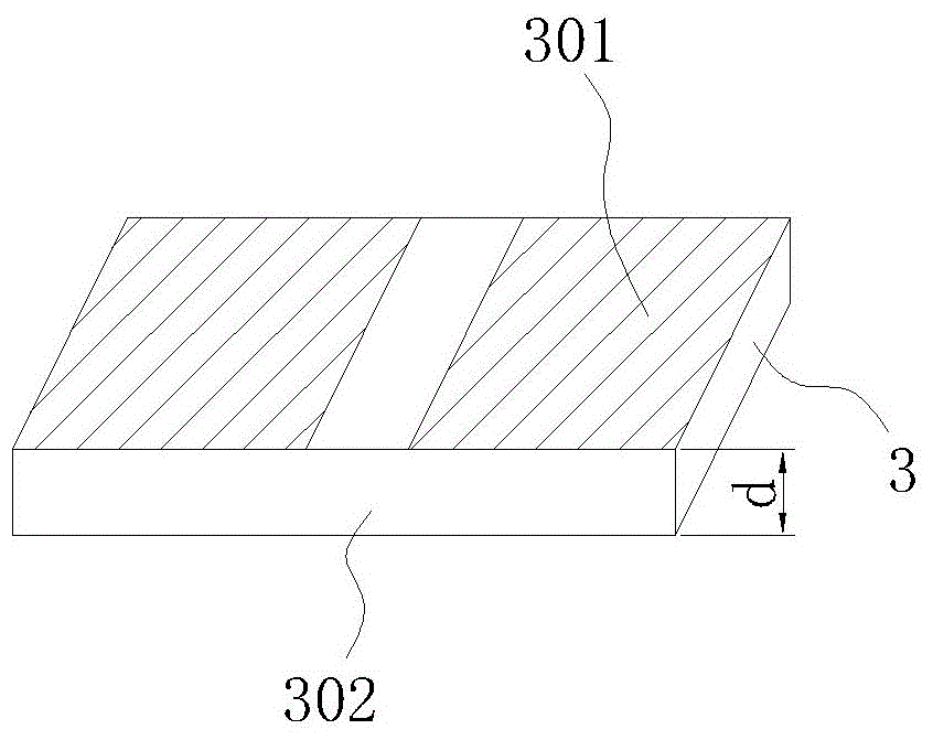
[0027] refer to Figure 1 to Figure 7 and Figure 8 As shown, the manufacturing method of the LED packaging structure proposed by the present invention includes:

[0028] S1, making brackets: using light-transmitting...


PUM


Abstract

The invention relates to the technology of LED packaging, and provides an LED packaging structure comprising light-transmitting supports, fluorescent glue and inverted LED chips. Each light-transmitting support is provided with a groove. The fluorescent glue at least covers the bottom surfaces of the grooves of the light-transmitting supports. The inverted LED chips are fixed on the fluorescent glue in a way that the light-emitting surfaces of the inverted LED chips face the direction of the grooves, and the electrode surfaces of the inverted LED chips are back to the direction of the grooves. The invention also provides a manufacturing method of the LED packaging structure. The manufacturing method comprises the steps that S1, the supports are manufactured: light-transmitting material is selected to manufacture the supports, and one groove is formed on each support; S2, the fluorescent glue is adhered; the fluorescent glue is adhered in the grooves of the supports; S3, drying is performed: the fluorescent glue in the grooves of the supports is solidified by drying; and S4, die-bonding is performed: the inverted LED chips are selected and are fixed on the fluorescent glue in the way that the light-emitting surfaces of inverted LED chips face the direction of the grooves, and the electrode surfaces of the inverted LED chips are back to the direction of the grooves. The LED packaging structure is used for packaging the LED chips so that packaging thermal resistance is substantially reduced.

Description

technical field [0001] The invention relates to the field of light emitting diodes (LEDs, Light Emitting Diodes), in particular to LED packaging technology. Background technique [0002] With the development of science and technology, LED lights have been widely used in various lighting fields due to their advantages such as high luminous efficiency, low power consumption, no need for high voltage, and high safety. The life of the LED light source is directly related to the working temperature of the node. At present, only about 50% of the electric energy of the LED lamp is converted into light energy during the working process, and the rest of the electric energy is almost converted into heat energy, which makes the temperature of the LED lamp rise. Reliability is halved for every 10°C increase in temperature. Heat dissipation is a big problem. If the heat dissipation is not good, it will directly lead to the decrease of LED performance and stability. At the same time, if...

Claims


Application Information

Patent Timeline
Patent Type & Authority Patents(China)
IPC IPC(8): H01L33/48H01L33/64H01L33/50H01L33/00H01L33/52
CPCH01L33/005H01L33/486H01L33/502H01L33/52H01L33/64H01L2933/0008H01L2933/0033H01L2933/0041H01L2933/005H01L2933/0075
Inventor 郑剑飞
Owner 厦门多彩光电子科技有限公司
Why Eureka
Try Eureka