Packaging structure and manufacturing method of a high-current power semiconductor device

A technology of power semiconductors and packaging structures, which is applied in semiconductor/solid-state device manufacturing, semiconductor devices, semiconductor/solid-state device components, etc. It can solve problems such as loss of resistance and thermal conductivity, virtual welding, frame deformation, etc., and achieve one-time The effect of processing and molding, simple process method, and reduced packaging resistance

Active Publication Date: 2019-10-11
WUXI NCE POWER
View PDF7 Cites 0 Cited by
  • Summary
  • Abstract
  • Description
  • Claims
  • Application Information

AI Technical Summary

Problems solved by technology

[0004] 1. In order to meet the high voltage or high current output, the emitter of the IGBT and the source of the MOSFET are often welded with multiple thick aluminum wires as connecting wires; the gate bears a small current, and thinner gold wires and copper wires are often used. Wires, alloy wires or aluminum wires are used as connecting wires; in this way, for the same package form, different metal leads need to be used, and lead frames or welding tools with different plating layers need to be selected according to the type of metal leads, and the aluminum wire machine itself is expensive. , which will result in waste of raw materials and high production costs;
[0005] 2. For some MOSFETs and IGBTs, the surface of the chip is divided into several parts by the gate bar. Considering the uniformity of the wiring of the power device, and the design of the lead frame limits the position and angle of the lead welding, it will cause There is no way to solder aluminum wire jumpers;
[0006] 3. Since the aluminum wire is difficult to form into a ball, cold wedge welding is generally used. Wedge welding uses the transducer to expand and contract rapidly under the induction of an ultra-high frequency magnetic field to generate elastic vibration, so that the steel nozzle (Wedge tool) vibrates accordingly, and at the same time, the steel A certain pressure is exerted on the nozzle, so under the joint action of these two forces, the steel nozzle drives the aluminum wire to rub rapidly on the surface of the aluminum metallized layer in the welded area, causing plastic deformation of the aluminum wire and the surface of the metal electrode to achieve the welding effect , repeated wedge welding of the same chip will increase the chance of dark cracks and craters inside the chip. In addition, the thickness of the steel nozzle (Wedge tool) is relatively large, and the area of ​​the pin welding area is limited. In actual production, multiple welding in the same area Difficult, and easy to cause virtual soldering, affecting the yield of packaging and product reliability;
Although the characteristics and reliability of the product have been significantly improved, special design is required for the part where the metal strip is connected to the frame, and it is easy to cause deformation of some relatively thin frames, resulting in flashing in the subsequent encapsulation process. The most important thing is This approach will still cause some loss of electrical resistance and thermal conductivity due to lead frame soldering
[0013] As mentioned above, there are many problems in the packaging of high-current and high-power semiconductor devices. The traditional packaging structure uses metal wires or metal strips to weld the semiconductor device and the pins. This structure has a large parasitic resistance and thermal resistance of the package, which affects the packaged device. The electrical characteristics and thermal performance, and the reliability is low, etc.

Method used


Image

  • Packaging structure and manufacturing method of a high-current power semiconductor device
  • Packaging structure and manufacturing method of a high-current power semiconductor device
  • Packaging structure and manufacturing method of a high-current power semiconductor device

Examples


Embodiment 1

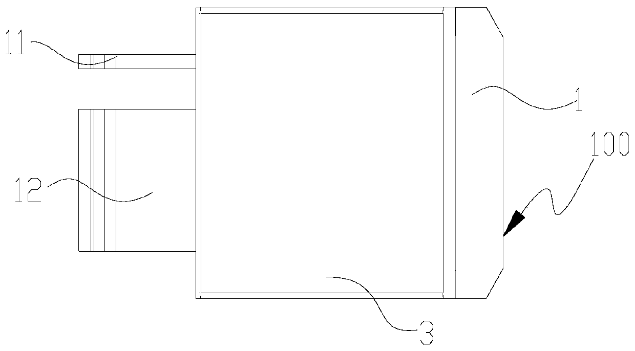
[0054] Embodiment 1 is package 100 SMD package form, image 3 and Figure 4 They are the front view and the rear view of the package 100 respectively. It can be seen from the figure that the semiconductor package 100 has two pins, which are the first conductive metal sheet 11 and the second conductive metal sheet 12 respectively, and the heat sink exposed at the bottom of the plastic package 3 1 is connected to the mounting base island 13, which can be regarded as the same component, and is made of the same material and the same processing technology, all of which are thermally and electrically conductive metal materials, such as copper, copper alloy, iron-nickel, aluminum, aluminum alloy, or Other conductive materials can also be understood as a component. The name and relationship between the heat sink 1 and the base island 13 are well known to engineers and technicians in the industry, so I won’t make too many descriptions here;

[0055] Figure 5 It is a perspective stru...

Embodiment 2

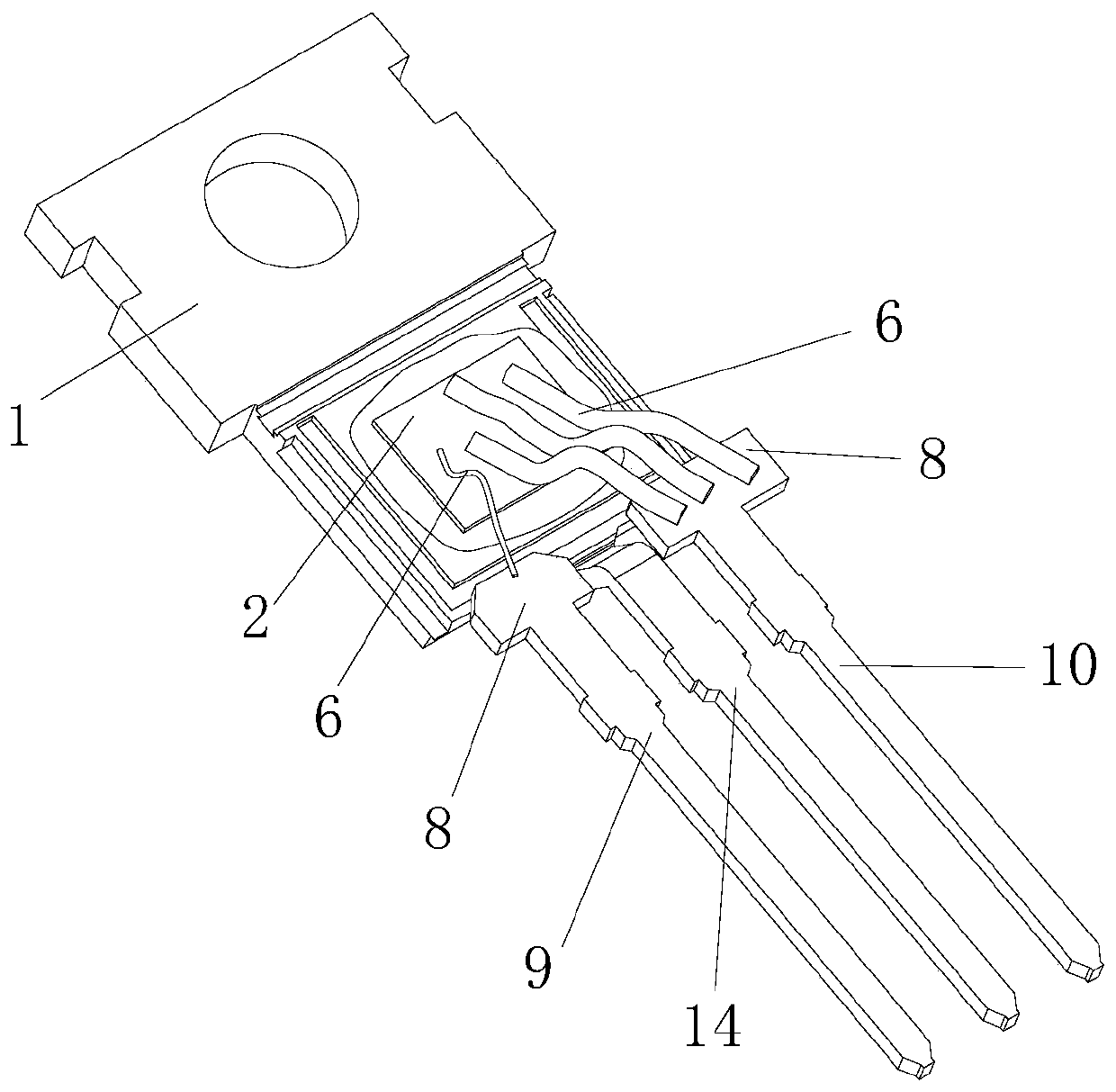
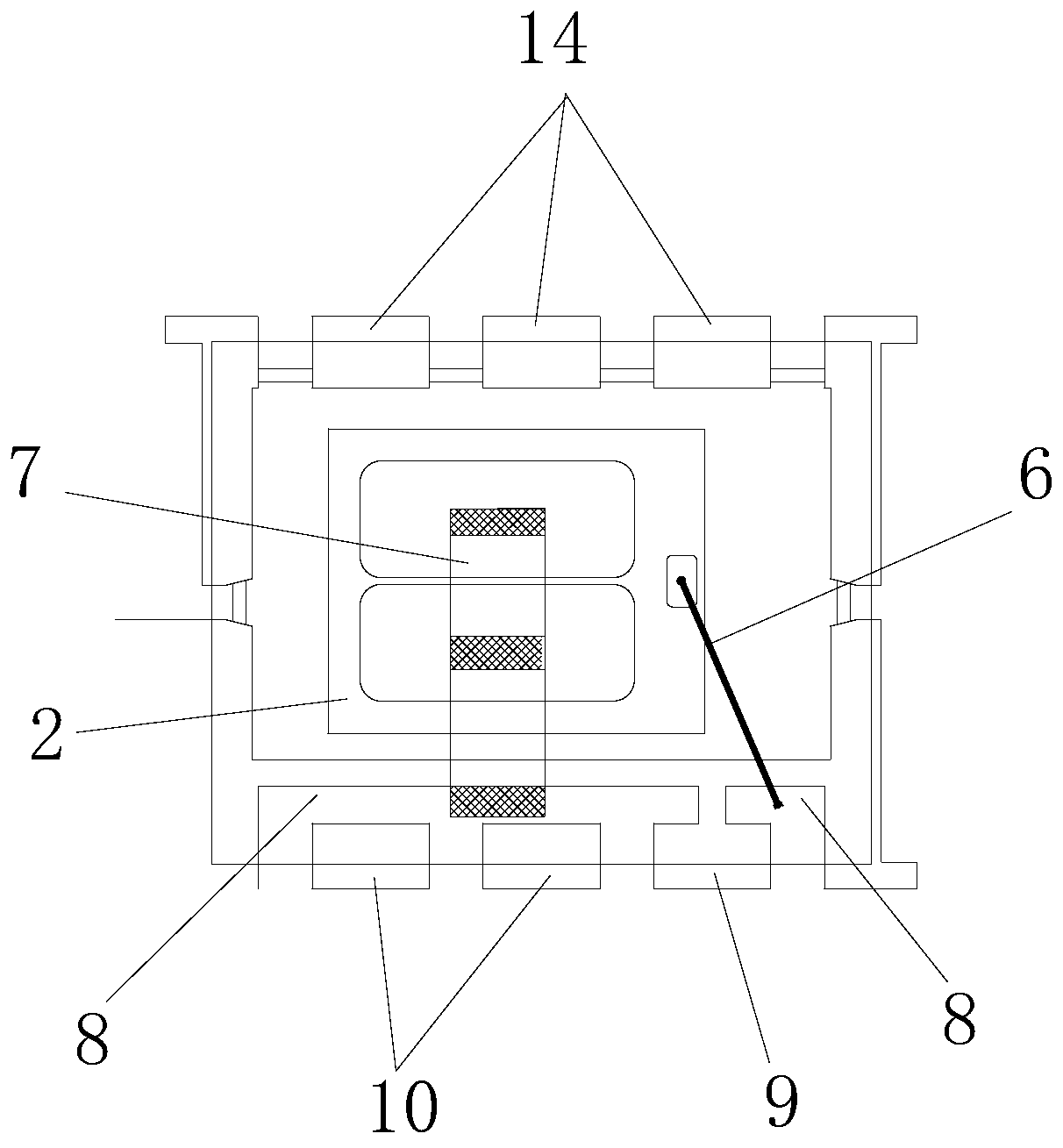
[0066] Embodiment 2 is in the form of package 200 in-line package, Figure 7 and Figure 8 They are the front view and the rear view of the package 200 respectively. From the front view, it is no different from the traditional TO-220, but from the rear view, the package 200 of this embodiment is different from the traditional TO-220 (such as figure 1 ) In contrast, the third electrode pin 14 of the package 200 is directly connected to the mounting base island 13 and is in the same plane, while the third electrode pin 14 of the traditional TO-220 is drawn out through the welding area 8 of the lead frame, and the mounting base The part of the island 13 and the third electrode pin 14 exposed outside the plastic package is not on the same plane.

[0067] like Figure 9 and 10 As shown, they are the internal structure and exploded view of the package 200 respectively. For the sake of simplification, the solder material has been omitted. The first conductive metal sheet 11 is use...

Embodiment 3

[0068] Embodiment 3 is an in-line packaging form of the package 300. In order to further improve the heat dissipation performance of the package 200, reduce the thermal resistance between the junctions, increase the current capacity, and reduce power loss, we thin the plastic package 3, and the second The bent portion 121 of the conductive metal sheet 12 is exposed outside the plastic package 3, such as Figure 12 and Figure 13 As shown, it is the appearance diagram and cross-sectional view of the package 300. Its structure is basically similar to that of the package 200. The main difference is that the thickness of the plastic package body 3 is only 1 / 5~1 / 2 of the original. Part of the second surface 132 and the heat sink 1 is exposed outside the plastic package 3, and the bent part 121 of the second conductive metal sheet 12 on the upper part is also exposed outside the plastic package 3, which achieves the effect of heat dissipation on both sides. The thermal resistance of...


PUM


Abstract

The invention relates to a packaging structure and manufacturing method of a high-current power semiconductor device, which includes a heat sink, a semiconductor chip, a plastic package body and a chip mounting base island, the chip mounting base island is connected to the heat sink, and the third electrode on the back of the semiconductor chip is welded to the mounting plate. On the first surface of the substrate island, it is characterized in that the first electrode on the front side of the semiconductor chip is welded to one end of the first conductive metal sheet, the second electrode is welded to one end of the second conductive metal sheet, and the substrate island is packaged in the plastic package. The first surface, the semiconductor chip, the welding ends of the first and second conductive metal sheets, the heat sink, the second surface of the base island, and the other ends of the first and second conductive metal sheets are all exposed outside the plastic package as pins The present invention uses conductive metal sheets as pins to be directly welded with the electrodes of the semiconductor chip, which not only reduces the device packaging resistance, increases the device overcurrent capability, but also enhances the heat dissipation capability of the device, reduces the package thermal resistance, and improves the reliability of the device package.

Description

technical field [0001] The invention relates to a packaging structure of a semiconductor device, in particular to a packaging structure of a high-current power semiconductor device, which belongs to the technical field of manufacturing semiconductor devices. Background technique [0002] High-current and high-power semiconductor devices are constantly developing. Silicon-based trench semiconductor chips have entered the 1mR era. The packaging resistance of traditional semiconductor device packaging structures accounts for a large proportion of the overall resistance, sometimes exceeding the internal resistance of the chip itself. , In addition, the packaging thermal resistance of semiconductor devices is relatively large, and the packaging thermal resistance determines the maximum power loss of the device. If the packaging thermal resistance and parasitic resistance can be effectively reduced, the current capability and power of MOSFET and IGBT devices can be improved. There...

Claims


Application Information

Patent Timeline
Patent Type & Authority Patents(China)
IPC IPC(8): H01L23/49H01L21/60
CPCH01L24/45H01L24/85H01L2224/4501H01L2224/85H01L2224/83801H01L2224/84801H01L2224/0603H01L2224/40H01L2224/48247H01L2224/4903H01L2224/49111H01L2924/13091H01L2924/13055H01L2924/00
Inventor 朱袁正朱久桃余传武陈慧玲
Owner WUXI NCE POWER
Why Eureka
Try Eureka