VDMOS (Vertical Double-diffusion Metal Oxide Semiconductor Structure) device and manufacturing method thereof
A device manufacturing method and device technology, which are used in semiconductor/solid-state device manufacturing, semiconductor devices, electrical components, etc., can solve the problems of low theoretical value of VDMOS device electrical properties, improve electrical properties, reduce on-resistance, improve The effect of utilization
- Summary
- Abstract
- Description
- Claims
- Application Information
AI Technical Summary
Problems solved by technology
Method used
Image
Examples
Embodiment 1
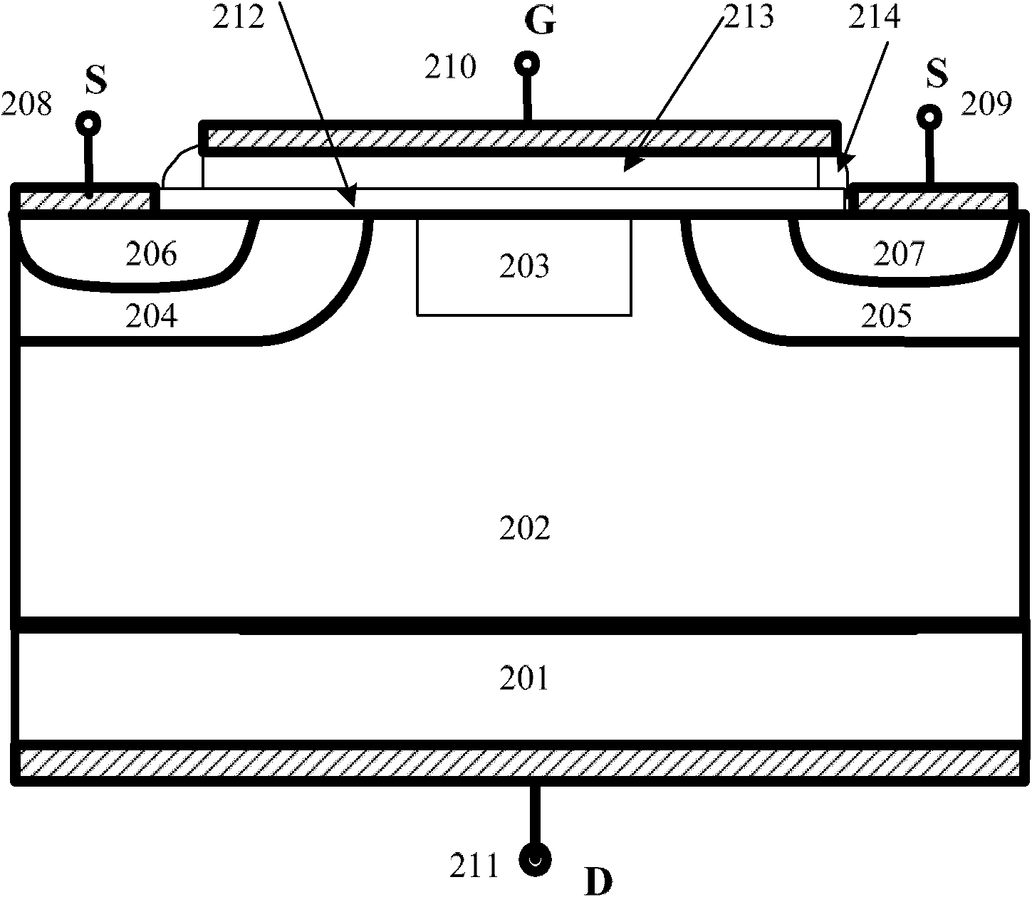
[0046] Based on this, the first embodiment of the present invention provides a VDMOS device whose structure is as follows figure 2 Shown, including:
[0047] A substrate, the substrate includes a body layer 201 and an epitaxial layer 202 located on the body layer, and the body layer includes a drain region;
[0048] The isolation region 203 located in the epitaxial layer 202. Generally, the isolation region 203 is located in the surface of the epitaxial layer 202, and there is no isolation region material on the surface of the epitaxial layer 202;
[0049] The first body region 204 and the second body region 205 in the epitaxial layer located on both sides of the isolation region 203, the doping state of the first body region 204 and the second body region 205 is the same as that of the epitaxial layer The conductivity type of doped ions is opposite;
[0050] The first source region 206 located in the first body region 204, the second source region 207 located in the second body regi...
Embodiment 2
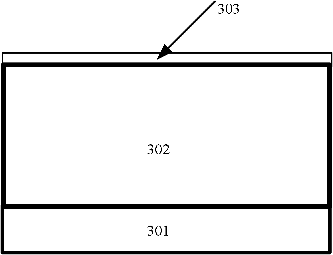
[0064] This embodiment discloses the manufacturing method of the VDMOS device described in the previous embodiment, Figure 3 to Figure 12 For the cross-sectional view of each step of the method, this embodiment only takes an N-type VDMOS device as an example for description. The method includes the following steps:
[0065] Such as image 3 As shown, a substrate is provided. The substrate includes a body layer 301 and an epitaxial layer 302 on the body layer 301. The body layer 301 includes a drain region. The body layer 301 and the epitaxial layer 302 in this embodiment are N-type doped ;
[0066] It should be noted that the substrate in this embodiment may include semiconductor elements, such as silicon or silicon germanium (SiGe) with a single crystal, polycrystalline or amorphous structure, or a mixed semiconductor structure, such as silicon carbide and indium antimonide. , Lead telluride, indium arsenide, indium phosphide, gallium arsenide or gallium antimonide, alloy semicon...
Embodiment 3
[0092] The manufacturing method of the VDMOS device disclosed in this embodiment is different from the method of forming the isolation region in the previous embodiment. In this embodiment, the step of forming the isolation region in the surface of the epitaxial layer includes:
[0093] Step 1: forming an opening in the surface of the epitaxial layer;
[0094] In this embodiment, a photolithography process can be used to form a pattern of openings on the surface of the epitaxial layer, and then the photoresist layer with the openings is used as a mask to etch away the epitaxial layer material at the openings to form a pattern on the surface of the epitaxial layer. Form an opening.
[0095] Step 2: Cover the surface of the epitaxial layer with an isolation layer to fill the opening with isolation layer material;
[0096] In this embodiment, chemical vapor deposition or physical vapor deposition may be used to cover the surface of the epitaxial layer with an isolation layer, and HDP (Hi...
PUM
| Property | Measurement | Unit |
|---|---|---|
| Thickness | aaaaa | aaaaa |
Abstract
Description
Claims
Application Information
 - Generate Ideas
- Intellectual Property
- Life Sciences
- Materials
- Tech Scout
- Unparalleled Data Quality
- Higher Quality Content
- 60% Fewer Hallucinations
Browse by: Latest US Patents, China's latest patents, Technical Efficacy Thesaurus, Application Domain, Technology Topic, Popular Technical Reports.
© 2025 PatSnap. All rights reserved.Legal|Privacy policy|Modern Slavery Act Transparency Statement|Sitemap|About US| Contact US: help@patsnap.com


