Boron-doped diamond micro-nano material with columnar array structure and preparation method thereof
An array structure and boron doping technology, applied in the field of micro-nano materials, can solve the problems of destroying the boron-doped diamond crystal plane structure, lack of controllability, poor order of silicon nanowires, etc., and achieve simple preparation process and realization Controllable, Widely Applicable Effects
- Summary
- Abstract
- Description
- Claims
- Application Information
AI Technical Summary
Problems solved by technology
Method used
Image
Examples
Embodiment 1
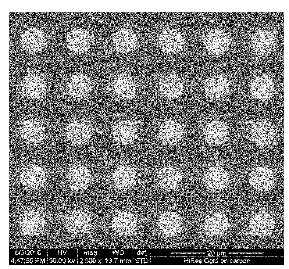
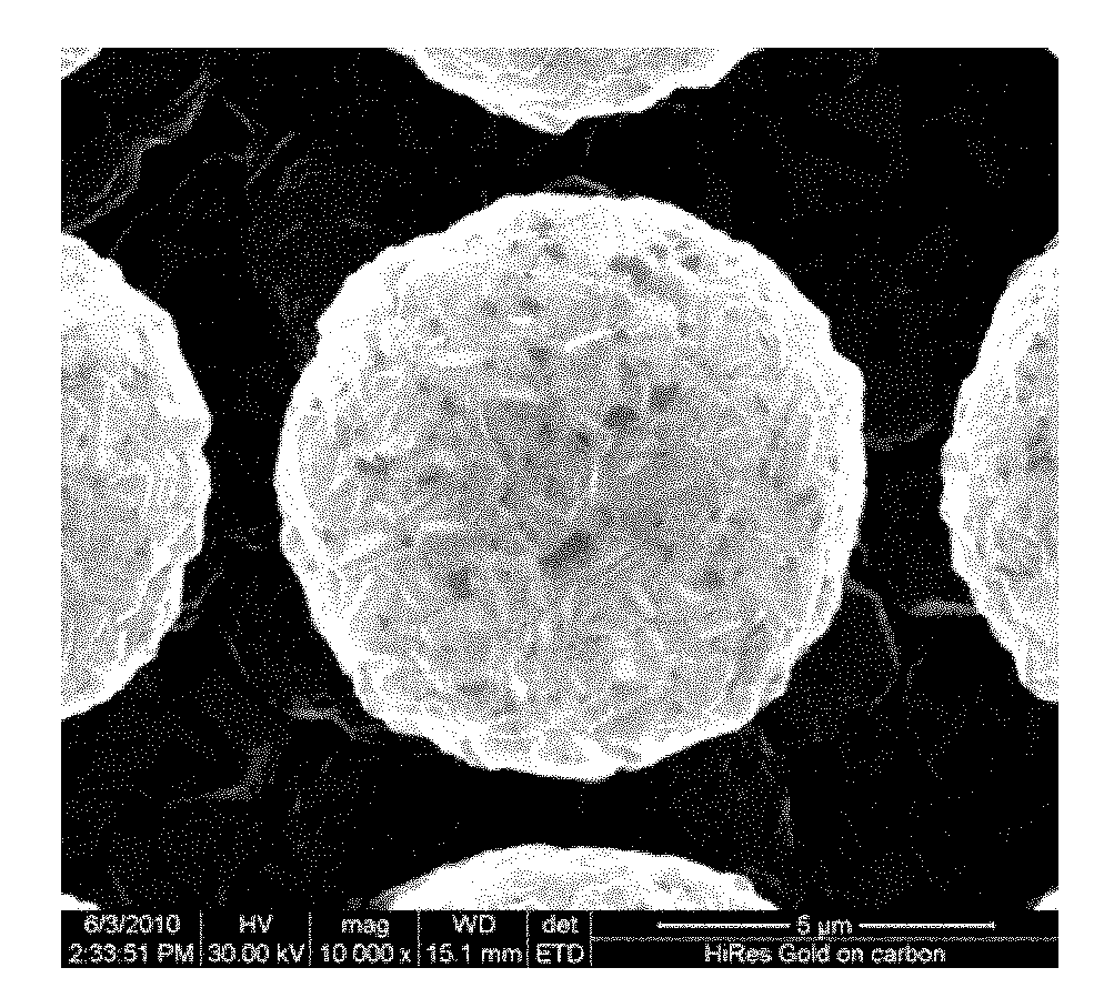
[0028] Example 1, a boron-doped diamond micro-nano material with a columnar array structure was prepared on a columnar array silicon substrate with a column height of 10 μm, a diameter of 5 μm, and a column spacing of 5 μm.
[0029] The production steps are as follows:
[0030] The first step is to select silicon with a crystal plane of (111), first oxidize the silicon surface to form an oxide layer, then spin-coat a photoresist coating on the surface of the oxide layer, expose and develop with ultraviolet light under the mask, and make the photoresist The coating forms a pattern corresponding to the mask pattern, and then uses inductively coupled plasma dry etching, first with C 4 f 4 Gas etched SiO 2 , then use SF 6 and C 4 f 8 Gas alternately etches Si to form a columnar array structure of silicon, and finally removes residual SiO with hydrofluoric acid solution 2 , to prepare a highly ordered columnar array of silicon, and adjust the height of the array column by cha...
Embodiment 2
[0035] Example 2, a boron-doped diamond micro-nano material with a columnar array structure was prepared on a columnar array silicon substrate with a column height of 5 μm, a diameter of 1 μm, and a column spacing of 2 μm.
[0036] The production steps are as follows:
[0037] In the first step, silicon with a crystal plane of (101) is selected, and the same method as in Example 1 is used to prepare a silicon substrate with a columnar array structure with a column height of 5 μm, a diameter of 1 μm, and a column spacing of 2 μm;
[0038] In the second step, the silicon wafer prepared in step 1 is cut into small pieces, cleaned, and ultrasonically inoculated with acetone-dispersed diamond seeds. The diamond seed solution is 0.5g of diamond powder dispersed in 100mL of acetone, and the inoculation time is 30min;
[0039] The third step is to place the silicon substrate inoculated with diamond seeds on the platform in the microwave plasma chemical vapor deposition reaction chambe...
Embodiment 3
[0042] Example 3, a boron-doped diamond micro-nano material with a columnar array structure was prepared on a columnar array silicon substrate with a column height of 20 μm, a diameter of 10 μm, and a column spacing of 10 μm.
[0043] The production steps are as follows:
[0044] In the first step, silicon with a crystal plane of (110) is selected, and the same method as in Example 1 is used to prepare a silicon substrate with a columnar array structure with a column height of 20 μm, a diameter of 10 μm, and a distance between columns of 10 μm;
[0045] In the second step, the silicon wafer prepared in step 1 is cut, cleaned, and ultrasonically inoculated with acetone-dispersed diamond seeds. The diamond seed solution is 5g of diamond powder dispersed in 100mL of acetone, and the inoculation time is 10min;
[0046] In the third step, the silicon substrate inoculated with diamond seeds is placed on the platform in the microwave plasma chemical vapor deposition reaction chamber,...
PUM
| Property | Measurement | Unit |
|---|---|---|
| thickness | aaaaa | aaaaa |
| height | aaaaa | aaaaa |
| diameter | aaaaa | aaaaa |
Abstract
Description
Claims
Application Information
 - R&D
- Intellectual Property
- Life Sciences
- Materials
- Tech Scout
- Unparalleled Data Quality
- Higher Quality Content
- 60% Fewer Hallucinations
Browse by: Latest US Patents, China's latest patents, Technical Efficacy Thesaurus, Application Domain, Technology Topic, Popular Technical Reports.
© 2025 PatSnap. All rights reserved.Legal|Privacy policy|Modern Slavery Act Transparency Statement|Sitemap|About US| Contact US: help@patsnap.com


