A preparation method of high-performance heat-radiating semiconductor planar light source
A planar light source and semiconductor technology, applied in the direction of semiconductor devices, semiconductor devices of light-emitting elements, light sources, etc., can solve the problems of poor heat transfer performance of LED light sources, reduced luminous efficiency of chips, and poor reliability of light sources, etc., to facilitate heat dissipation , Reliability and life improvement, and the effect of reducing light loss
- Summary
- Abstract
- Description
- Claims
- Application Information
AI Technical Summary
Problems solved by technology
Method used
Image
Examples
Embodiment 1
[0021] Mix and stir 10g of 100nm-10μm diamond particles, 100g of polyethylene glycol and 50g of silica gel to form a slurry;
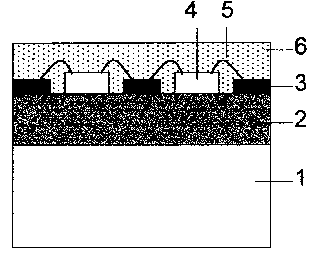
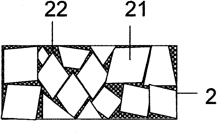
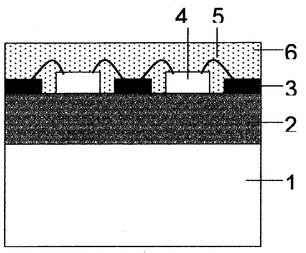
[0022] Print the composite paste on the surface of the aluminum substrate 1 by screen printing, heat it to 300-400°C in a vacuum environment, and keep the temperature for 1-2h, and form a dense diamond film 2 after the organic components in the paste volatilize , after high temperature treatment, the film thickness is about 20-30μm, such as figure 2 As shown, the insulating high thermal conductivity diamond film 2 is composed of large diamond particles 21 with a thermal conductivity of 1000-2000W / K*m and a particle size of 0.1-10 μm, and large diamond particles 21 filled with particles of a particle size of 1-100nm small diamond particles 22, so that the diamond film 2 is dense, and the thermal conductivity between the large diamond particles 22 can be enhanced;
[0023] Use the conductive silver paste to print on the surface of the aluminum-based di...
Embodiment 2
[0027] 8g of diamond particles of 250nm-5μm are mixed with 80g of polyethylene glycol and 100g of silica gel to form a slurry;
[0028] Print this slurry on the surface of the aluminum substrate 1 by using the traditional scraping method, heat it to 200-300°C in the atmosphere, and keep the temperature for 0.5-1.5h. The organic components in the composite slurry volatilize to form a dense diamond film. 2. After high temperature treatment, the thickness of diamond film is about 15-20μm;
[0029] A copper film is directly deposited on the surface of the aluminum-based diamond film 2 as the conductive layer 3 by magnetron sputtering and other techniques, and then according to the circuit design, the required circuit pattern is obtained by etching.
[0030] The LED chip 4 is directly welded on the surface of the diamond film 2 at the hollowed-out part of the conductive layer 3 in the designed composite aluminum substrate, and then the positive and negative electrodes of the LED ch...
PUM
| Property | Measurement | Unit |
|---|---|---|
| particle diameter | aaaaa | aaaaa |
| particle diameter | aaaaa | aaaaa |
| thickness | aaaaa | aaaaa |
Abstract
Description
Claims
Application Information
 - R&D
- Intellectual Property
- Life Sciences
- Materials
- Tech Scout
- Unparalleled Data Quality
- Higher Quality Content
- 60% Fewer Hallucinations
Browse by: Latest US Patents, China's latest patents, Technical Efficacy Thesaurus, Application Domain, Technology Topic, Popular Technical Reports.
© 2025 PatSnap. All rights reserved.Legal|Privacy policy|Modern Slavery Act Transparency Statement|Sitemap|About US| Contact US: help@patsnap.com


