Photoelectric integrated packaging structure based on low temperature co-fired ceramics

A technology of low-temperature co-fired ceramics and optoelectronic integration, applied in laser devices, semiconductor laser devices, circuits, etc., can solve the problems of non-penetrating special-shaped structure design, inability to carry out special-shaped design, and limited integration, etc., to achieve Contribute to large-scale production, improve integration and reliability, and simplify the effect of packaging process steps

Active Publication Date: 2021-02-12
INST OF SEMICONDUCTORS - CHINESE ACAD OF SCI
View PDF8 Cites 0 Cited by
  • Summary
  • Abstract
  • Description
  • Claims
  • Application Information

AI Technical Summary

Problems solved by technology

[0003] In array integration, the traditional ceramic thin film circuit can only be designed in a single layer, so when designing a slot structure or a via hole, it can only penetrate the entire board, and it is impossible to design a non-penetrating special-shaped structure; for a double-layer structure , can only be supported by pads between layers. Obviously, the reliability of this method is relatively low, the volume increases, and special-shaped design cannot be carried out, which limits the improvement of integration.
If it is a structure with more than two layers, the traditional method is not competent, and the LTCC process can only be used for chemical molding preparation

Method used


Image

  • Photoelectric integrated packaging structure based on low temperature co-fired ceramics
  • Photoelectric integrated packaging structure based on low temperature co-fired ceramics
  • Photoelectric integrated packaging structure based on low temperature co-fired ceramics

Examples


Embodiment Construction

[0048] In order to make the object, technical solution and advantages of the present invention clearer, the present invention will be further described in detail below in conjunction with specific embodiments and with reference to the accompanying drawings.

[0049] Regarding the "first", "second", "third"... etc. used herein, it does not refer to the meaning of sequence or sequence, nor is it used to limit the present invention, but it is only for the purpose of distinguishing The term describes the element or operation only.

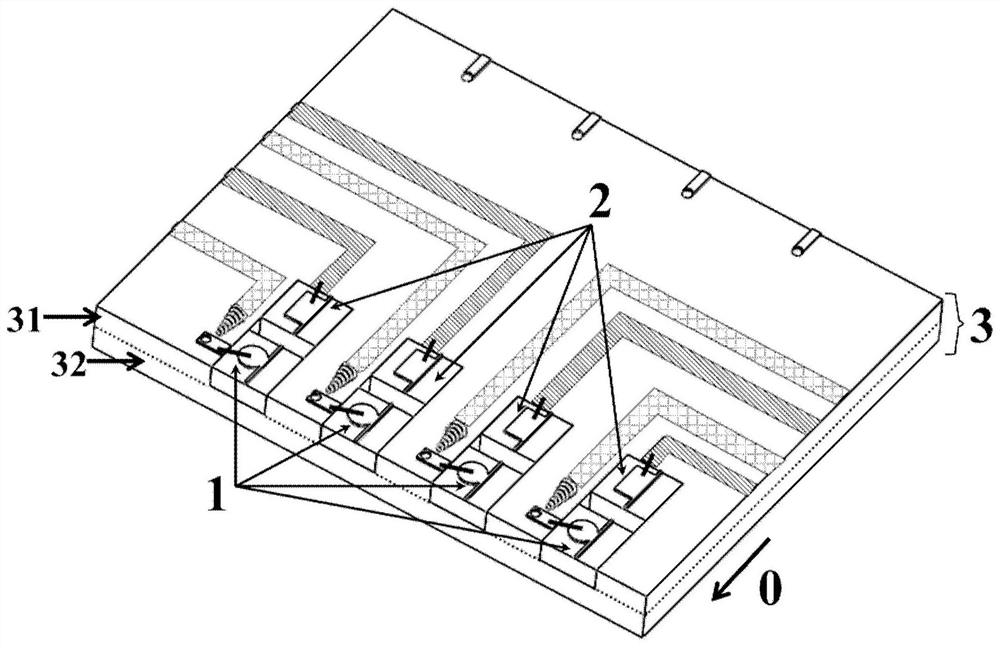
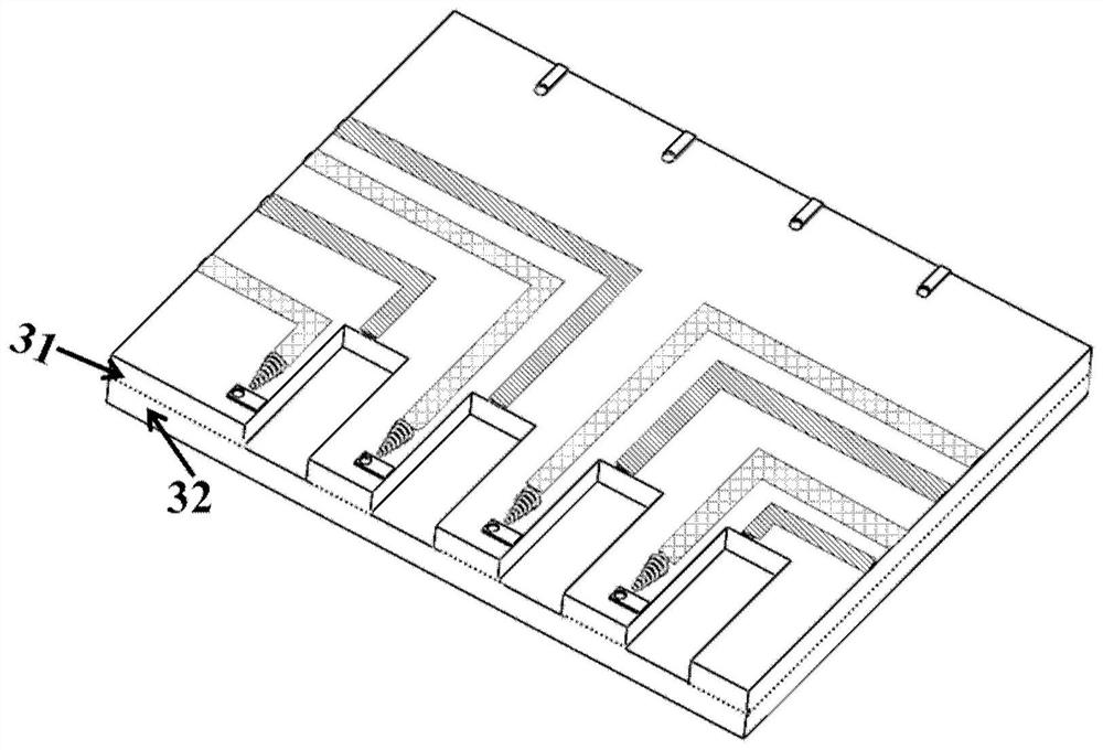
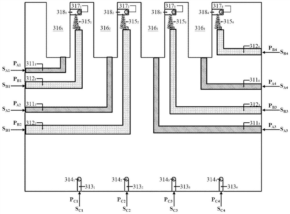
[0050] In order to solve technical problems such as low reliability, large volume, and limited integration caused by the connection between layers through pads, the present invention proposes an optoelectronic integrated packaging structure based on low-temperature co-fired ceramics. Structures include:

[0051] The invention provides an optoelectronic integrated packaging structure based on low temperature co-fired ceramics, including:

[0052] A mu...


PUM


Abstract

The invention discloses a photoelectric integrated packaging structure based on a low-temperature co-fired ceramic. The photoelectric integrated packaging structure comprises a multifunctional low-temperature co-fired ceramic substrate (3), a backlight detector chip array (2) and a laser chip array (1). The multifunctional low-temperature co-fired ceramic substrate (3) at least comprises a high-frequency functional layer (32) used for transmitting high-frequency signals and a direct-current functional layer (31) used for transmitting direct-current signals (31) from bottom to top; the backlight detector chip array (2) comprises N backlight detector chips; and the laser chip array (1) comprises N laser chips. According to the photoelectric integrated packaging structure based on the low-temperature co-fired ceramic, a plurality of functional layers are laminated integrally through a low-temperature co-fired ceramic technology to form the low-temperature co-fired ceramic substrate, and a three-dimensional circuit diagram is formed in the substrate through a via hole structure; signal transmission is achieved; and the photoelectric integrated packaging structure has the characteristics of high reliability, high integration level, small size and the like, and is suitable for integrated packaging of large-scale high-density array chips.

Description

technical field [0001] The invention belongs to the field of optoelectronic / microelectronic devices, and more specifically relates to an optoelectronic integrated packaging structure based on low temperature co-fired ceramics (Low Temperature Co-fired Ceramic, LTCC). Background technique [0002] For high-speed laser chips, their normal operation needs to be loaded with DC signals and high-frequency signals at the same time. At the same time, in order to facilitate adjustment, it is often necessary to separate the DC path and the high frequency path. [0003] In array integration, the traditional ceramic thin film circuit can only be designed in a single layer, so when designing a slot structure or a via hole, it can only penetrate the entire board, and it is impossible to design a non-penetrating special-shaped structure; for a double-layer structure , can only be supported by pads between layers. Obviously, the reliability of this method is relatively low, the volume incr...

Claims


Application Information

Patent Timeline
Patent Type & Authority Patents(China)
IPC IPC(8): H01S5/40H01S5/02335H01S5/0232
CPCH01S5/4025H01S5/02345H01S5/02355
Inventor 张志珂韩雪妍赵泽平郭锦锦刘建国
Owner INST OF SEMICONDUCTORS - CHINESE ACAD OF SCI
Why Eureka
Try Eureka